

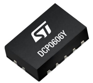
The DCP0606Y is ST’s first high-current synchronous automotive 6 V-6 A step-down converter. As carmakers offer heads-up displays, digital assistants, and cameras, among other features, they must deliver far greater efficiency across all loads. The DCP0606Y offers a typical 93% efficiency at 2.25 MHz with nearly 100% duty cycle to help meet these new demands. However, engineers can also double its switching frequency to 4.4 MHz to reduce inductor sizes and lower the bill of materials. Designers thus have far greater flexibility. For instance, they can use the low-consumption mode at 2.2 MHz to avoid interference with audio bands while using higher frequencies when working with a digital processor.
DCP0606Y: A unique approach that nearly triples efficiency
The new demands for electrical efficiency
The new demands, driven by head-up displays and infotainment systems, require engineers to seek continuous high-current converters with incredible efficiency. This is something quite new, since carmakers really didn’t ask for such a device five years ago. They did offer heads-up displays, multimedia applications, and cameras, but didn’t need to push efficiency that far. However, as zonal architectures are reshaping car platforms and makers look to lower the overall weight of cars or increase the battery life of electric vehicles, increasing efficiency has become the new Eldorado. And to meet this challenge, we married our expertise in power management and automotive-grade manufacturing to offer a solution so unique that we are patenting it.
The new dual-control-lopp architecture
The DCP0606Y is unique because it features an innovative dual-control-loop architecture that maintains high efficiency regardless of the load. In essence, a constant time loop ensures a low quiescent current (about 10 µA) when experiencing a light load, while a peak current mode manages to keep the noise down at high load conditions by maintaining a constant frequency and fast transient response. And to ensure optimal performance, the new ST regulator dynamically switches between the low-consumption mode (LCM) and the low-noise mode (LNM). Engineers can also force either by acting on the MODE/SIN pin.
The new normal: efficiency in numbers
To further the efficiency of the new device, ST used a low RDS(ON) MOSFET rated at 11 mΩ for the high-side and low-side. Concretely, the ST component has a typical quiescent current and a maximum shutdown current that is almost three times lower than that of some of its most direct competitors. The DCP0606Y can also regulate the output voltage from 0.6 V to 6 V with an accuracy of ±1.5% across line, load, and temperature conditions. Moreover, designers can set the typical switching frequency between 1.8 MHz and 4 MHz by using an external resistor connected to the FSET pin, making the new device quite flexible, as it can fit a wide range of designs.
DCP0606Y: A great package and way to get started
The next design
The DCP0606Y stands out thanks to its QFN 2 mm x 3 mm package, which is smaller than the competition’s. It also uses wettable flanks to enable production lines to employ optical inspection to check solder quality, rather than X-rays, which is necessary when the pads are hidden underneath. Similarly, engineers can use a multi-layer PCB approach to dissipate heat through the VIN and GND pins. The DCP0606Y thus necessitates only passive cooling, and as long as designers follow our layout considerations, they will easily minimize electromagnetic interference and other noises. Additionally, ST will ensure that future DCP060xY devices are pin-to-pin compatible, enabling teams to reuse their designs.
The next project
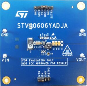
The best way to get started is to grab the STEVAL-0606YADJ, an evaluation board that can serve as an implementation example, since we provide the schematics and Gerber files. The board will offer a 3.3 V – 6 A output at 2.25 MHz. It also includes EMI filters. The STEVAL-0606YADJ also includes test points to monitor certain features. For instance, when linking VIN and MODE points using the provided jumper, users can force the LNM mode while binding MODE and GND triggers the LCM mode. It’s also possible to use the SOUT pin to synchronize three DCP0606Y units, simplifying the overall design when powering multiple units within an SoC, such as the CPU, GPU, and RAM.