

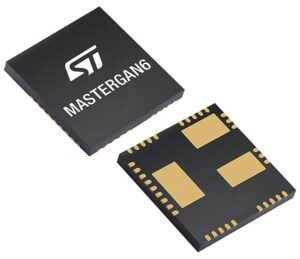
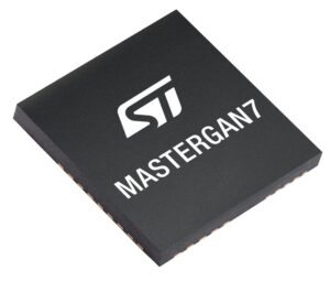
The MASTERGAN6 and MASTERGAN7 are the first ST GaN power devices to include LDOs, rather than relying on external ones, and the first to offer a hard-switching topology capable of tolerating negative voltages as low as -6 V in hard-switching topologies, making the new series more integrated and more robust. As a result, designers can create systems with significantly greater power density while enjoying a simpler bill of materials and high switching frequencies. As GaN makes its way into more chargers, adapters, or solar panels, to name a few, MASTERGAN6 and MASTERGAN7 are important steps in its democratization. Both devices are nearly identical except for a higher RDS(ON) on the latter.
Why GaN can be a challenge to use?
Engineers are forced to choose between power density and reliability
It’s clear that gallium nitride is a key material in the quest to increase power density. Consumers see it in chargers that continue to deliver more watts in smaller form factors, with some mass-market models delivering up to 800 W total by offering multiple charging ports, with some supporting 240 W on a single USB-C PD port. However, there’s a slew of new designs that get less attention from the general public but profit from GaN’s properties, such as automotive-grade power supplies, power inverters for solar panels, server and data center systems, and much more. For many of these, reliability is as critical as, if not more so than, power density.
The challenge is that improving power density and reliability simultaneously is a tall order. Using a material like GaN drastically improves power density thanks to its wide bandgap (3.39 eV) and its ability to offer high electron mobility when mixed with nitrogen (1,700 cm2/Vs). However, designers then have the task of driving the new material, which gives the most advantages at switching frequencies above 200 kHz and entails its own set of obstacles, such as hard-switching tolerance, cross-conduction protection to prevent a short between the high side and ground, and overall gate robustness. This explains why the industry remains bullish on GaN adoption but never expected an overnight move from silicon power devices.
It demands a new design philosophy
A corollary to the inherent challenges of adopting Gallium Nitride is that it demands a whole new design philosophy. As a result, makers must not only provide power devices but also an entire platform to guide designers on their journey. That means reference designs, simulation software, PCB layout wizards, and more. Unfortunately, while many compete on devices, few provide the support, tools, and development boards that can significantly speed up a proof of concept or lower the barrier to entry. Although GaN devices offer higher power density, engineers still have to manage thermal constraints within smaller footprints while maintaining the same overall reliability. Better models and design tools can help with that.
How MASTERGAN6 and MASTERGAN7 solve these challenges?
Integrated LDO for robustness
MASTERGAN6 and MASTERGAN7 address the new design challenges by incorporating two LDOs for both the high-side and low-side drivers. Concretely, the new design helps reduce the bill of materials by eliminating the need for an external power supply for the drivers. It also makes the new ST devices compatible with a broader range of controllers. Moreover, the integrated LDO helps with gate robustness, a common issue in GaN devices, because the power device must be driven with a precise voltage without excessive oscillation, to avoid risks of damaging the gate. The LDO helps provide greater stability and can, therefore, address common GaN issues.
New dedicated pins for energy efficiency and greater control
The two new devices introduce a dedicated standby-shutdown pin. It helps improve energy efficiency by enabling the MCU to enter a low-power mode immediately. In a nutshell, it’s possible to keep MASTERGAN6 and MASTERGAN7 off or in a state that requires very little current longer, thanks to a pin that offers significantly more control over the device’s behavior. Similarly, a pin to adjust the dV/dt of the transistor via an external resistor enables engineers to reduce electromagnetic interference. Basically, ST aims for greater efficiency, robustness, and control over our GaN power devices.
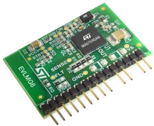
An advanced development platform
The best way to get started is to grab the EVLMG6 half-bridge power module. It can be mounted on top of an STNRG599 board and use the SRK2001A controller to demonstrate a resonant LLC converter. The solution is relatively small and can help developers rapidly implement the new features of the MASTERGAN6 and MASTERGAN7. Indeed, this evaluation platform features a power density of 34.5 W/in3. As a result, engineers can even draw inspiration from our schematics for their layouts or use the PCB Thermal Simulator to develop their designs faster.