

Update, March 9, 2026
About a year after our original announcement (see original publication below), ST is thrilled to announce that the PIC100 technology is now entering high-volume production on 300 mm wafers. We anticipate quadrupling our production by 2027 to meet the massive demand for silicon photonics technology that supports higher bandwidth and energy efficiency for hyperscalers’ AI workloads. Finally, we shared last year that we were working on a PIC100 using through-silicon via, and are now unveiling a concrete PIC100-TSV technology roadmap. By using ultra-short vertical electrical connections, ST can support a much denser module and support near- and co-packaged optics. It will also enable us to create technologies capable of addressing 400 Gbps/lane.
Original publication, February 20, 2025
The PIC100 is ST’s first silicon photonics technology and one of the most efficient PICs on a 300 mm wafer, thus enabling 200Gbps/lane and even greater bandwidth in the future. Indeed, this is a highly symbolic launch as it inaugurates a long series of PICs that will bring new efficiencies to data centers, AI clusters, and other optical networking appliances. ST knows the market well since many pluggable optical transceivers are already using our BiCMOS B55. By launching a more efficient PIC and a next-generation B55X using silicon germanium and a 55 nm process node, makers of pluggable transceivers can provide new efficiency ratings and performance, which are essential for the democratization of faster communication standards.
PIC100: Performance, efficiency, and scalability
The problem of heat dissipation
Anyone who has ever dealt with fiber communication technologies knows that pluggable optical transceivers can get very hot, very quickly. In fact, pluggable modules have seen their aggregate power consumption steadily increase over the last few years due to the upscaling of their aggregate bandwidth. Therefore, as bandwidth increases significantly, it becomes much harder to keep temperatures and power consumption in check. The problem is that while servers need higher data throughput for AI and other data-intensive applications, high heat can cause serious challenges, including performance degradation and reliability issues. Moreover, as data centers strive to be more sustainable and power-efficient, hotter and more power-hungry optical transceivers run counter to these objectives.
PIC100’s solutions to lower losses
To improve efficiency and optimize the optical link budget for advanced pluggable transceivers, the PIC100 features single-mode silicon waveguide loss down to 0.4 dB/cm and single-mode silicon nitride waveguide loss as low as 0.5 dB/cm across both O- and C-bands. Moreover, the PIC100 offers Mach-Zehnder Modulator (MZM) electro-optical bandwidth capability of 50 GHz and a high-speed photodetector up to 80 GHz. Put simply, the PIC100 is unique because it integrates all these devices into a single 300 mm stack.
Efficiency is also the reason we adopted an edge-coupler-compatible PIC100 stack. Many in the industry tend to adopt grating couplers because they help reduce costs during testing and the initial alignment process. For instance, grating couplers enable wafer-level testing and offer more flexible placement. However, they suffer from greater losses due to greater scattering and a more significant optical mode mismatch between the coupler and the fiber. By leveraging the PIC100 patented stack, we can better match the fiber mode to the on-chip SiN waveguide, resulting in far more efficient coupling with losses well below 1dB.
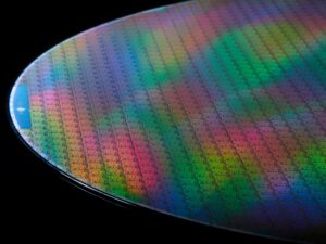
ST’s 300 mm fab
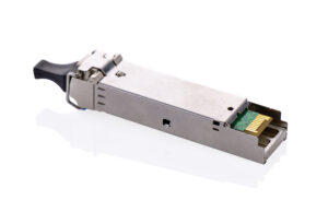
ST customers are already working on 800 Gbps and 1.6 Tbps pluggable modules, making today’s PIC100 launch meaningful as they ramp up in the second half of 2025. This announcement thus marks the beginning of a new era, as transceiver makers are already fully leveraging the benefits of ST’s PIC platform for 200 Gbps/lane pluggable transceivers. It also clearly explains why AWS is already working with ST, and the leading optical module provider, to adopt PIC100 in their data centers.
ST’s PIC: looking at the future of silicon photonics in data centers
An easier upgrade path toward 1.6 Tbps transceivers
ST customers are already working on 800Gb/s and 1.6Tb/s pluggable modules, making today’s PIC100 launch meaningful while ramping up from the second half of 2025. This announcement thus marks the beginning of a new era, as makers are already taking advantage of ST’s PIC to 200Gbps/lane pluggable transceivers. As these QSFP56 modules have suffered from shortages, our new device should help alleviate these issues and provide an intermediate step between 100G and 400G interfaces, thus enabling data centers to upgrade their infrastructure gradually. It also explains why AWS is already working with ST and the leading optical module provider to use the PIC100 in their data centers.
A roadmap towards 400 Gbps/lane and GPU-x optical links
While we are not providing any release dates at this point, we are committed to creating PICs supporting 400 Gbps/lane that will scale alongside the next-generation data centers. As AI trains on GPUs’ massive parallelism, this demands a constant and tremendous need for bandwidth, making the creation of faster and more power-efficient transceivers a top priority. Hence, pluggable module makers can be assured that they can continue sourcing their PIC from ST for many generations to come.
Finally, ST is announcing the release of the BiCMOS B55X. The successor of the B55 will further improve efficiency thanks to its use of silicon germanium and a 55-nm process node. Compared to a system that uses only a PIC100 with a competing BiCMOS chip, code signing both the PIC100 and the B55X chips will increase efficiency by about 15%. ST is also working on a through-silicon-via (TSV) module and compact modulators to enable the use of our ST PIC100 in GPU-to-X optical interconnection, thereby enabling high-speed communication in scale-up and scale-out optical engines for Near- and Co-Packaged Optics applications.