

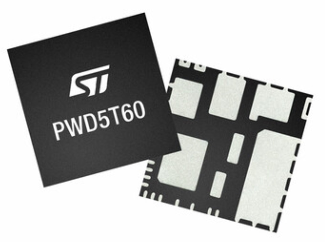
SiP, or system-in-package, technology is experiencing strong adoption, with many studies anticipating double-digit growth over the next five years, thanks in part to its unique electrical properties and the ability to use dies of different sizes under one roof, also known as heterogeneous integration. ST is part of this movement with devices like the PWD13F60, PWD5F60, PWD5T60 power drivers, or the powerSTEP01 microstepping controller leading the charge. However, we are also seeing that assembly lines are often less familiar with this technology, leading to a closer partnership that helps them overcome common issues. Hence, we thought it was a good time to review some manufacturing fundamentals around SiP integration.
SiP challenge #1: Reliable joints
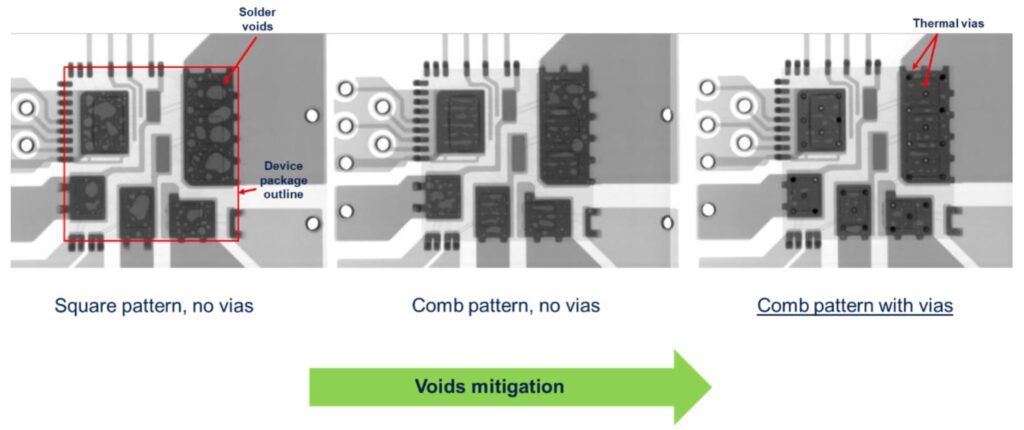
The problem with voids
The most common concern is the creation of reliable joints that are free of voids. Indeed, simply applying paste and heating the device isn’t optimal because it’s easy for a SiP to have misalignment, for excessive solder paste to bridge two patches, or for trapped gases to create pockets of voids during reflow. These gaps are a problem because they cause overheating due to poor heat dissipation and lead to reduced yields. This is even more of a problem given that SiP devices feature large exposed pads for heat dissipation. Traditional guidelines from the IPC (Institute of Printed Circuits) recommend that voids do not exceed 50% of the exposed pads’ area, which can be difficult without proper processes.
Comb pattern
The first solution ST recommends is going back to strong fundamentals by keeping packages in a moisture-barrier bag and ensuring ESD-safe environments. It may sound simplistic, but no workaround will help if moisture plagues an assembly line. The next step is to choose the right stencil for the job. Instead of using full patterns (a large square mimicking the exposed pads’ dimensions) or a square pattern (little squares filling the area), a comb pattern with a 300 µm opening and a 600 µm pitch provides the best results. According to the IPC, any exposed pad larger than 4 mm x 4 mm should use a pattern. Hence, using the right one is critical.
Drilling vias
The other critical solution is the use of vias about 0.25 mm in diameter, spaced 1 mm apart, and uniformly placed around the pad, to allow air gases in the flux to escape. Larger vias would suck in too much paste, and smaller vias would provide diminishing returns. In our application note AN6217, we even show X-ray images of the underside of a SiP package to demonstrate the benefits of a comb-pattern-with-vias approach. The document also covers other considerations, such as proper reflow soldering and the best solder paste (type 4 is often preferred, but type 3 works). But a proper stencil and via structure go a long way.
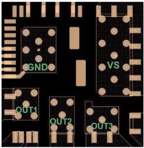
SiP challenge #2: Effective layout and heat dissipation
Obsoleteness of old guidelines
SiP packages are attractive because they are unique. They can house many different dies in a slim package, reducing the overall footprint of diverse devices on the PCB and simplifying the design. To make this possible, a SiP employs numerous techniques such as interposers, redistribution layers, bridges, and more. That means engineers must treat them differently. They don’t usually take a heatsink (none of our devices do), and they most often dissipate energy through their bottom pads. Consequently, they need to be laid out differently on the PCB than traditional packages. Simply reusing design guidelines from other packages will result in overheating, shorts, and poor reliability.
Creating dissipating islands and using a four-layer PCB
One of our most common recommendations to manufacturers is to create “dissipating islands”, which are thick layers of copper on the PCB under the exposed pads to better conduct heat away from its source. It’s basically made-up heatsinks that engineers can connect through vias for greater dissipation. The number of copper layers will also depend on the PCB layer count. Hence, it might be worth considering moving from a two-layer to a four-layer structure. While the PCB becomes more expensive to produce, it allows designers to use the more cost-effective SiP and improve overall density while meeting dissipation goals, thereby lowering total costs.
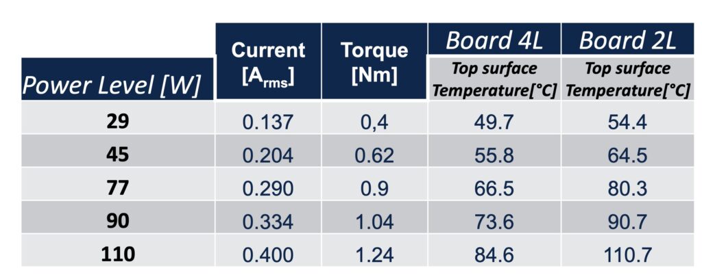
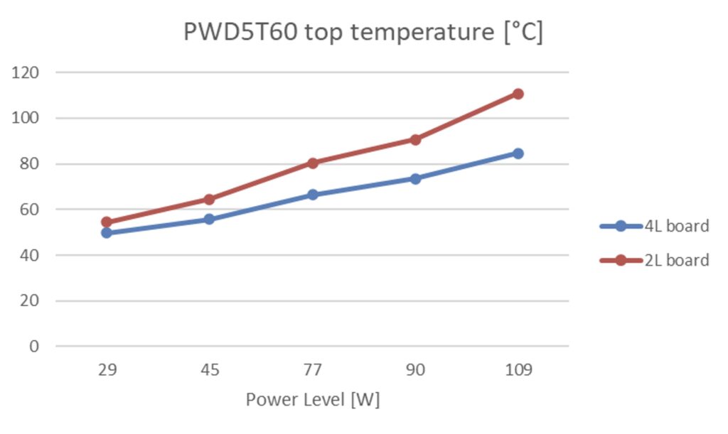
In fact, we ran internal benchmarks using the PWD5T60 to show the effects of moving from four layers to two when designing a fan motor. At 29 W, moving to four layers reduces the top surface temperature of the ST device by 8.6%, while at 110 W, the difference is more than 30%. And while the PWD5T60 was still operating within the rated junction temperature of 125 ºC, it was getting awfully close to its limits. In fact, in a separate compressor motor design, the two-layer PCB wouldn’t handle 90 W. Hence, engineers can gain significant benefits by switching to more layers, and exploring a thicker PCB can pay considerable dividends.
New electrical considerations
There are other layout considerations to take into account, such as the ground connection. As the microcontroller drives the SiP’s power stage, it’s critical to connect the ground point to the shunt resistor to limit voltage spikes. We also recommend connecting all ground pads and exposed pads to a solid ground plane directly under the power components and above the signal layer to shield against electromagnetic interference. Placing the bulk capacitor as close to the SiP as possible and decoupling capacitors as close to the supply rail pin will also lower parasitic inductance and resistance. Ultimately, these considerations are pretty straightforward, and keeping them in mind can vastly reduce a project’s time to market.