

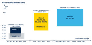
The STWA60N028T is the first STMESH superjunction MOSFET to use a deep trench approach and to be manufactured on a 12-inch wafer. As a result, it features a low RDS(on) of 28 mΩ and supports a drain-source voltage (VDS of 600 V), thus putting the new device in the same medium-to-high-voltage category as our MDmesh M6 and MDmesh M9 series while offering a cost-effective price structure thanks to the larger wafer and new lithographic techniques that have enabled us to be vastly more efficient. The new trench design only requires half the mask layers as the previous devices, and involves significantly fewer steps.
ST in the trenches
Why superjunctions
Avid readers of the ST Blog will remember that on the 20th anniversary of MDmesh, we alluded to the fact that we were working on deep trench technologies. It would allow the creation of a P column in a single step, thus shortening and simplifying production to make superjunction MOSFETs more accessible. In general, creating this column in the epitaxial layer between the P and N semiconductors creates a superjuction that lowers the RDS(on) by a factor of 4, thus enabling very high voltages without incurring outrageous temperatures or losses. As such, when medical or telecommunication products need very rugged devices, they often turn to superjunction MOSFETs instead of wide-bandgap devices.
Why multi-epitaxial and deep trenches
Until now, all ST superjunction MOSFETs have used a multi-epitaxial approach, and we will continue to employ this technique on numerous devices, as it still yields excellent results. In a nutshell, in this method, multiple masks are used to etch the trench and then grow epitaxial layers before doping them. In early generations, the doping process would create a circular pattern. Over time, the industry figured out how to build thinner trenches and reduce the out-diffusion pattern, thus improving the device’s electrical properties. However, the process necessarily involves numerous steps and masks, which explains why a deep trench approach is very attractive. The issue was surmounting the manufacturing challenges that come with digging such a trench.
The STWA60N028T reaching 96.9% power efficiency
The benefits of moving to deep trenches and 12-inch wafers
The STMESH Trench Technology, which allows the creation of a P column in a single step, represents a new era for our family of superjunction MOSFETs. The STWA60N028T is also highly symbolic because it’s the first STMESH device we manufacture on a 12-inch wafer, which is viable because the lithographic processes we use yield excellent results. Consequently, customers can expect shorter cycle times since we can produce more of the new device at once. And this is only the beginning. As ST continues to perfect concepts like multi-drain, which we find on the MDmesh M9 series, we can expect new superjunction MOSFETs.
The need for varied package types
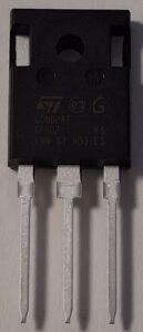
In the meantime, the STWA60N028T is not only unique for ST but comes in numerous packages (TO-247-LL, TO-LL, PFLAT 8×8, D2PAK, DPAK, SOT223–2) to fit a wide range of applications. The first devices will adopt a TO247LL housing, which is popular in telecommunication and server applications. We often see D2PAK in SMPS and SOT223 in home appliances. We will also offer versions with and without a fast recovery diode. As a result, we expect the STWA60N028T in products that need fast switching speeds, like switch-mode power supplies destined for demanding industrial appliances.
Additionally, thanks to its low RDS(on), it can boost efficiency by a couple of percentage points compared to an MDmesh M6, thus enabling makers to offer more power-efficient systems at a lower price point. Concretely, in our internal testing on a 1,500 W boost PFC, we obtained a peak efficiency of 96.9% at 600 W, thus surpassing all previous MDmesh devices and even most competing solutions. And now that the device is more cost-effective, we should see these numbers in a more significant number of applications needing up to 1,200 W, including more consumer-oriented systems.
- Learn more about the STWA60N028T