
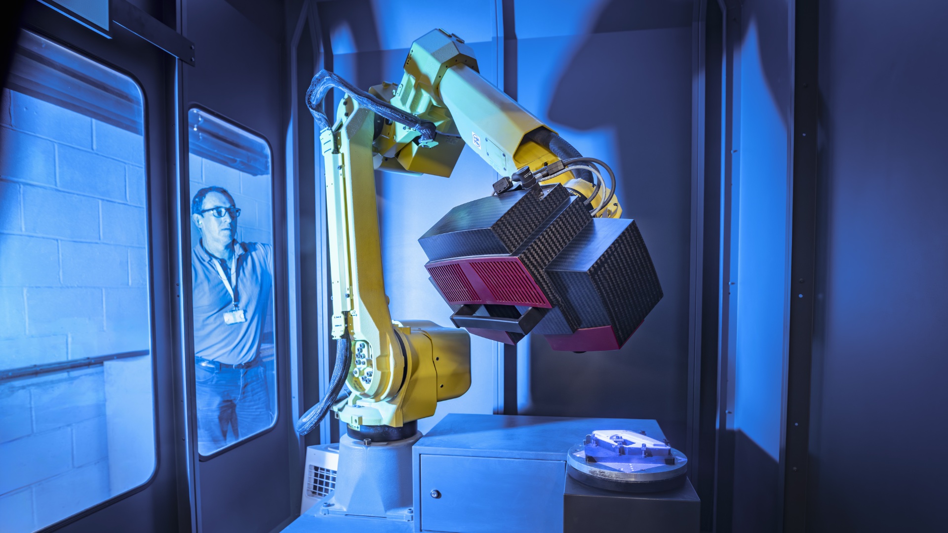
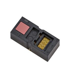
The VL53L9 is ST’s highest-resolution 3D Time-of-Flight LiDAR sensor, with up to 2.3K zones, and it’s also the first with dual-scan flood illumination, which stands out from competing dot illumination by better detecting smaller objects and edges. The new module has a field of view of 54º x 42º and a range from 5 centimeters to 9 meters. It can stream data at up to 100 Hz, and its low-power mode requires only 150 mW. The VL53L9 also aims to be future-proof as it’s our first ToF to support MIPI and I3C interfaces. Put simply, it meets the new demands from AR/VR, drones, or humanoid robots for more accessible 3D depth mapping.
Why is 3D depth mapping still a hard problem?
It is at the core of many applications
Applications like robotics and drones have a small footprint but also require small-object detection, which relies on high-resolution depth maps and a wide field of view. Similarly, people counting or fall detection in smart buildings is increasingly popular because their use of IR maps means it’s impossible to recognize a particular individual, and local computing capabilities imply that the information stays on the device, which is the ultimate privacy safeguard, but it also means that the system must run on low-power embedded systems. And AR/VR systems will only gain traction if they can correctly detect the smallest movements, which is only possible with a dense depth map.
It requires a high resolution
These considerations explain why engineers increasingly turn to all-in-one LiDAR modules. Companies no longer ask why products should use 3D depth mapping. They know it’s no longer an option. Five to ten years ago, companies were still mostly experimenting with gaming accessories, scanners, and very basic AR/VR systems. Today, with the advent of robotics, smart buildings, smart glasses, and physical AI, more and more systems need it, but sometimes struggle to use it. Indeed, too often, engineers don’t get the resolution they need for precise object or people tracking, or the lighting conditions are inadequate. There are not enough zones, so systems can’t properly track small objects, avoid tiny obstacles, or monitor subtle gestures.
It can be costly and complex
The solution to this problem is not very new, but it is very costly, as it mainly involves adding sensors. It also significantly increases complexity. Adding discrete LiDAR stacks entails challenging alignment and calibration issues. It also means a more complex PCB layout and a harder-to-manage BOM, since it involves more parts, sometimes from different vendors. There are also inherent limitations to such an approach, including a more restricted field of view and the use of dot illumination, which has a harder time detecting smaller objects because it provides fewer measurement points than flood illumination.
It is computationally expensive and power hungry
More resolution and more measurements mean greater computational needs. However, that involves upgrading the ASIC, as most competing sensors today can’t handle all these data points and would thus require offloading much of the computation to an external MCU. Unfortunately, that tends to strain standard interfaces, such as I2C, which can become a bottleneck. Needing a more powerful MCU and additional sensors also increases the overall power consumption. Sadly, many new applications that require a 3D ToF LiDAR sensor need greater efficiency, either because they are battery-powered or because they use a small form factor incompatible with heatsinks and large power supplies. Put simply, while we know that adding multiple sensors helps, it’s not always feasible.
VL53L9 or what are the new solutions engineers can count on?
2,300 zones and flood illumination
The VL53L9 tackles the resolution challenge by using multiple SPADs (Single Photon Avalanche Diodes) on a single module and a new meta-surface optical element, both of which enable higher resolution in a small package. Put simply, we added more sensing capabilities to one sensor. Consequently, having all these new data points transformed our device from a simple ToF measurement system into a full-on 3D depth-map LiDAR module. The VL53L9 is much more capable because it can capture much more data. Behind the scenes, this is possible because ST developed manufacturing optimizations that enabled us to pack more into a single device. Having everything on chip also eliminates the need for complex calibration.
A more powerful ASIC and faster interfaces
Similarly, the VL53L9 comes with a more powerful ASIC than previous generations of time-of-flight sensors. Concretely, it means the device can run far more complex algorithms and perform more advanced computations without relying on an external MCU. For instance, the VL53L9 can stream processed data, such as a 2D and depth multizone distance map, at 60 frames per second, the fastest fps for this type of sensor today. It can even reach up to 100 fps in a more basic streaming scenario and when using MIPI. We also provide optimizations, such as the ability to set different modes on the device based on whether detected objects are closer or farther than 1 meter.
All this translates into real-world benefits for new edge AI applications, as they now benefit from higher-quality data delivered at higher bandwidth, thanks to this new ASIC. While the industry understands the value of edge AI applications, as they offer greater privacy and run much more efficiently since all computations are local, engineers still heavily depend on the sensor’s performance. The new IC of the VL53L9 can process more data, reducing demands on the microcontroller and RAM and opening the door to more powerful edge AI applications that can run inference operations faster and with greater accuracy while using existing MCUs.
How to get started?
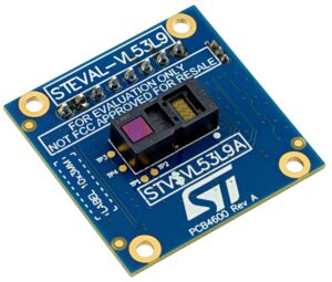
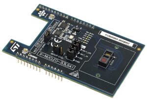
The best way to get started is to grab one of our development boards. The X-NUCLEO-53L9A1 features the VL53L9 and can fit an I3C-compatible Nucleo board like the NUCLEO-H563ZI or the NUCLEO-N657X0-Q. For those wishing to experiment with I3C and MIPI, we also offer the STEVAL-VL53L9 evaluation board, which can sit atop the NUCLEO-N657X0-Q or the STM32N6570-DK Discovery Kit. STM32CubeIDE has received updates to support all these configurations, and we even offer a graphical user interface that currently works with the X-NUCLEO-53L9A1 and NUCLEO-H563ZI to lower the barrier to entry and make edge AI applications that rely on depth maps more accessible.