The STM32H7 series of microcontrollers (MCU) made history today by becoming the most powerful implementation of the ARM® Cortex®-M7 processor for the embedded market. It is more than twice as fast as the STM32F7 series, the previous STM32 flagship series, meaning that its core frequency of 400 MHz has enabled ST to become the first ever to reach 2010 points in CoreMark with a Cortex-M MCU.
This is possible because ST is the first to have shrunk its M7 implementation from a 90 nm process node to 40 nm. Media outlets have recently reported that some manufacturers have started or are about to start mass producing SoCs in 10 nm. However, it is important to understand that these components only have digital circuits, unlike the embedded MCU from ST, which includes digital circuitry, Flash memory, and analog components. Hence, these structures are much more complex than typical mainstream components and thus require more complex processes. Therefore, the 40 nm node used today is not only groundbreaking but the gateway to a masterful implementation of the Cortex-M7, and although we can’t enumerate all the great updates or optimizations found in the STM32H7 in one single post, we’ve decided to focus on some of the reasons why its performance sets new records.
Three Domains, Memory-Packed

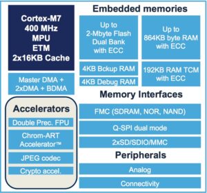
To optimize the STM32H7, its architecture has been divided into three domains. Very simply, the first one (D1) includes the core with its cache, Flash memory and high bandwidth peripherals like the module to drive a screen or the Chrom-Art graphics engine. D2, the connectivity domain, groups low-speed peripherals like USB, the cryptographic accelerator and the SD/MMC2 unit for storage. Finally, D3, the batch acquisition mode domain, is responsible for some of the most fundamental aspects of the MCU like its reset and clock control as well as ADCs, GPIO, RTC, the chip’s power management and a basic DMA (BDMA) controller.
This structure allowed ST to design a flexible and efficient architecture that packs a massive internal memory compared to some STM32F7 series. For instance, the L1 Cache is now four times bigger with 16 KB for instructions and the same amount for data. ST also included a total of 1 MB of SRAM and 2 MB of Flash, which is three times and twice as much respectively as the previous generation. However, instead of using a single block of SRAM, that would only benefit a certain domain, the STM32H7 placed various amounts at different locations to make the memory more versatile.
Concurrent Access

The D1 domain obviously holds the largest amount of SRAM. The core has a total of 192 KB of TCM SRAM (64 KB I-TCM, optimised for instructions and 128 KB D-TCM, optimised for data), which acts as an extension to the L1 cache. It has the same performance but is addressable. This means that TCM RAM can be accessed by the core with no latency and developers can specifically place information that needs to be deterministically retrieved to perform time-critical routines. The biggest chunk of SRAM (512 KB) is in the first domain because it contains the most computing intensive aspects of the architecture. Finally, D2 and D3 offer a quick access to their SRAM by the peripherals and other modules on the chip.
This organization has the great advantage of providing concurrent memory access, meaning that information can be fetched or stored in the different chunks of SRAM at the same time and by different domains, greatly improving the efficiency of the architecture. This is extremely important as embedded MCUs must often handle computationally intensive tasks, like running graphics and audio, while talking to an interface like a USB port to ensure that there is no disruption in the data transfer.
Optimized Memory and FPU
Another great feature stemming from the increased computational power of the STM32H7 series is the ability to use ECC SRAM and Flash. The speed increase compared to the STM32F7 series is so high that ST now has the computational resources to add error correction and still break performance records. By providing ECC, ST not only ensures data integrity, but also improves data retention in the Flash.
Another example of an architectural decision motivated by the needs of ST’s customers was the use of a double precision (FP64) floating point unit. The need for such a pipeline may not always be obvious, but some of the products that will benefit the most from the STM32H7 series need to perform DSP-type computations. For instance, an embedded system that monitors a power grid and will need to compute fast Fourier Transform algorithms, or a connected device that will run a precise GPS system will rely heavily on double precision computations.
Power Saving Features and So Much More

It is impossible to offer a comprehensive list of all the features and optimizations brought by the STM32H7 series in a single blog post. We haven’t even touched on the amazing power consumption optimizations that are offered by this three-domain architecture. For instance, it is possible to put D1 and D2 in a very low-powered standby mode (7µA) while D3 continues to capture data in its SRAM without needing to wake up the other domains, therefore greatly saving energy. There’s also a complex and elaborate clock-control scheme to ensure that different parts of the architecture run at varying speeds in order to further improve the MCU’s efficiency.
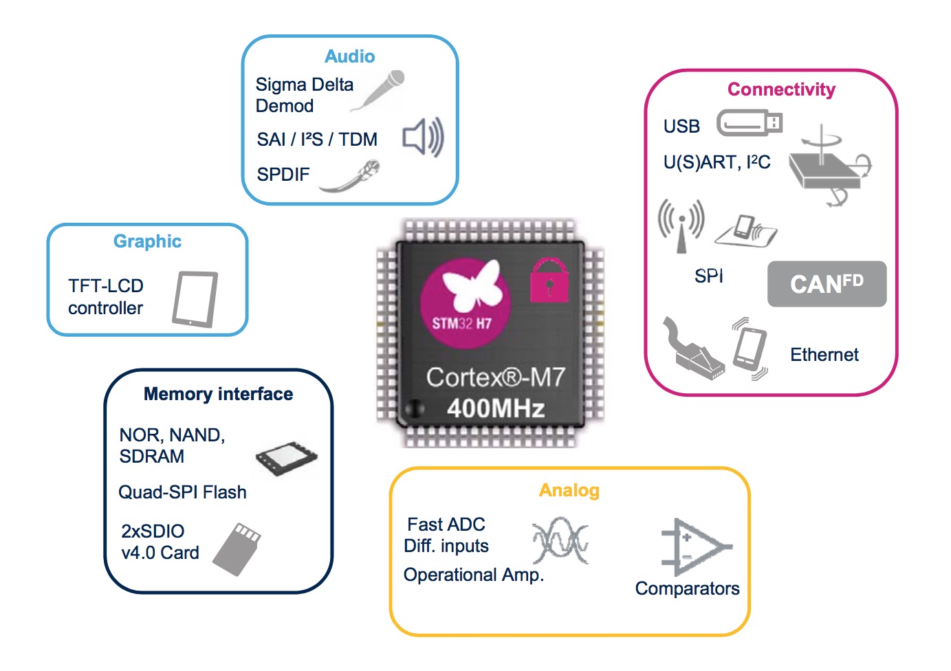
The STM32H7 series also builds on the previous generation by adding 10 more communication peripherals for a total of 35, it still offers cryptographic and hashing hardware acceleration, and remains pin to pin as well as software compatible with the STM32F7 series. The record-breaking STM32H7 series is sampling today to specific partners, and will be in mass production in Q2 2017. At this time, ST will have updated the mbed development platform to ensure developers can take full advantage of this groundbreaking architecture.
To know more about the STM32H7 series, please visit ST’s website.
