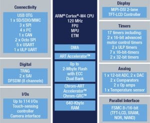
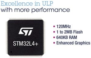
The new STM32L4+ launching today is the first family of microcontrollers (MCU) that scores more than 200 in ULPMark even though it has 640 KB of SRAM, 2 MB of Flash, and a Cortex-M4 running at a 120 MHz. It makes it one of the best power-to-performance ratios ever for this kind an ultra-low power MCU. Officially known as STM32L4Rxxx or STM32L4Sxxx, the STM32L4+ components also include a new Chrom-GRC engine and a MIPI DSI controller for displays, which explains why the new architecture targets smartwatches and other wearables, among many other devices such as industrial sensors, meters, home automation, and medical applications.
The classic STM32L4 is a favorite among manufacturers looking to use a lot of sensors while keeping consumption very low. One example is the heart rate monitor from Valencell that proved highly popular at the ST Developers Conference 2016 because it could compute sensor fusion algorithms using data from a SensorTile board while still fitting on a small wristband. Hence, STM32L4 MCUs currently rank in the top 5 of the ULPMark hall of fame, and the new STM32L4+ parts are unique because they keep the same philosophy centered on extreme efficiency while proving to be even more powerful thanks to several optimizations.
How Chrom-GRC Works?
One of these optimizations takes the form of Chrom-GRC (Graphics Resource Cutter). In a nutshell, it is a graphics memory management unit that’s so smart it can shrink the size of the frame buffer by up to 20 % when the device doesn’t use a rectangular display. Very simply, the frame buffer is the piece of RAM that stores the color value for each pixel that the user will end up seeing on the screen. One may think of it as a binary representation of the image to display before the system converts it into a video signal and sends it to the panel. Chrom-GRC’s prowess lies in its ability to adapt this data to the shape of the display to only store the visible pixels, automatically discarding those that can’t show up on the screen, therefore saving significant resources.
If we take as an example the approximately 1.2″ displays of the smartwatches that came out this year, which have a resolution of 390 x 390, we end up with an image made of precisely 152,100 pixels (3902). Since those screens have a color depth of 24 bit, we end up with a raw image size of 3,650,400 bits (152,100 x 24) or a frame buffer of about 446 KB (3,650,400 ÷ 8 ÷ 1024). However, because these MCUs don’t have a smart memory management system like the one in the STM32L4+, they store the entire image, including the bits the panel’s IC will discard because of the round shape of the display, for instance. Given that most systems also need 256 KB for applications, it’s easy to see why competing MCUs very often include 1 MB of SRAM.
How the STM32L4+ Drives Displays?
If we run the same simulation as above, but send the rendered image to new Chrom-GRC, the system will distinguish the pixels visible to the user from those that aren’t, then proceed to delete the latter and shrink the frame buffer by up to 20 %. Hence the image in memory no longer weighs 446 KB, but 357 KB. Also, as was the case for some STM32L4, the STM32L4+ embeds the Chrom-ART Accelerator (DMA2D), which optimizes certain graphics computations. By using the Chrom-ART engine, it is possible to relieve the main CPU of some repetitive 2D-graphic operations, such as 2D copies, transparency, or alpha blending. Other tasks, like pixel format conversions, are performed twice as fast as if they were done by the central processor.
The MCU then sends the frame to the display through a controller. The STM32L4+ still includes a TFT controller, but ST also integrated a MIPI DSI controller for engineers wishing to use a more modern interface. The Mobile Industry Processor Interface (MIPI, pronounced “mipee”) Display Serial Interface (DSI) is highly prevalent in mobile devices because it uses a fast and high-resolution data stream to communicate with the screen’s IC. The MIPI DSI controller in the STM32L4+ uses two lanes of up to 500 Mbit/s each. As a result, the host MCU can manage higher resolution displays while requiring less power, and fewer pins, as well as reduce electromagnetic interferences. All this is possible because the system serializes the pixel and command data into a single physical stream to optimize their transport.
Objectively More Efficient
At their core, the STM32L4+ MCUs are ultra-low power components. As such, they are impressive because their architecture only needs 43 µA/MHz, and shutdown mode requires just 33 nA. Furthermore, ST made the structure flexible by offering multiple sleep, standby, and stop methods to optimize power consumption whatever the user activity. For instance, the Stop 2 mode can keep the entire SRAM active, or shut down 384 KB (that could be assigned to the frame buffer for example) to only use the 256 KB dedicated to applications and data acquisitions from the sensors. Hence, if the screen and the frame buffer are off, as is often the case when a smartwatch is idle, this mode lowers the current to a mere 2.8 µA. Furthermore, since waking from a stop mode only takes 5 µs, there’s no perceivable penalty to the user.
However, it’s one thing to talk about power consumption, but it’s another to be validated publicly by an objective source, which is why ST is proud to announce that the STM32L4+ family scores 233 points in EEMBC’s ULPMark CP (Core Profile). Since no other MCU in the database comes close to its configuration, a comparison is difficult. Nevertheless, as a reference, we see that some competing chips with just 128 KB of SRAM and a Cortex M4 at 52 MHz only manage to get a score of 203 in ULPMark (bigger is better), and the MCU with the highest “Retention SRAM” only scores a mere 72 points. Similarly, the STM32L4+ has a high ULPMark PP (Peripheral Profile) score of 56.5, but since the top 5 MCU in this benchmark are all STM32L4, it ultimately means that ST beat its own device and moved the leaderboard further.
Experiencing the Power of the STM32L4+… Now!
It is impossible to exhaustively list in a single blog post all the features that make the STM32L4+ such a robust architecture. For instance, compared to the STM32L4 components that run at 80 MHz maximum, the new family can go up to 120 MHz, which puts the architecture in another league entirely. The STM32L4+ is also the first STM32 architecture to offer two Octo SPI ports, supporting NOR Flash (including execute-in-place) and HyperbusTM RAM. Ultimately, despite its typical run consumption of just 43 µA/MHz, the MCU can still reach 410.32 in Coremark and 150 DMIPS when running at its maximum frequency.
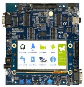
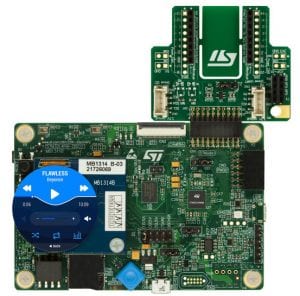
The best way to start experimenting with the STM32L4+ is to grab either its Nucleo Kit (NUCLEO-L4R5ZI), the Discovery Kit (STM32L4R9I-DISCO) or the evaluation board STM32L4R9I-EVAL. They each include the most powerful and feature-rich version of the architecture. Engineers and enthusiasts can thus start developing their applications and even further test the power consumption as well as run more ULPMark tests by using the recently launched STM32 Power Shield. It will then be faster to decide which exact STM32L4+ MCU fits best a specific design since they only really vary when it comes to pin count, Flash capacity, and the presence or absence of particular features.
Furthermore, since they are all pin-to-pin compatible, switching from one to another has never been so easy thanks to STM32CubeMX and STM32L4Cube. Finally, The STM32L4+ portfolio, as well as all the kits and boards, are in production now and we can’t wait to see how they will boost the creativity and innovation of our partners and our community.


