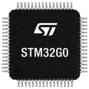
The STM32G0 is our newest family of mainstream microcontrollers (MCU) for cost-oriented consumer and industrial applications. This new generation offers a Cortex-M0+ core at 64 MHz as well as a robust architecture with a Securable Memory Area, more RAM and Flash, numerous I/Os, and a more extensive integration of components to simplify the overall PCB design significantly. As energy requirements from various regulatory bodies become more stringent, and users expect more from their IoT platforms, engineers often face the impossible task of choosing an MCU that must have a low power consumption, while also delivering computationally demanding features and encryption acceleration. As a result, they must either chose a lesser capable but lower-power model, or enjoy the I/Os they need, but deal with a much higher overall TDP (Thermal Design Power). The STM32G0 is here to solve this problem.
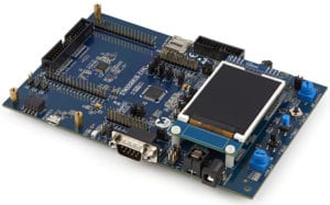
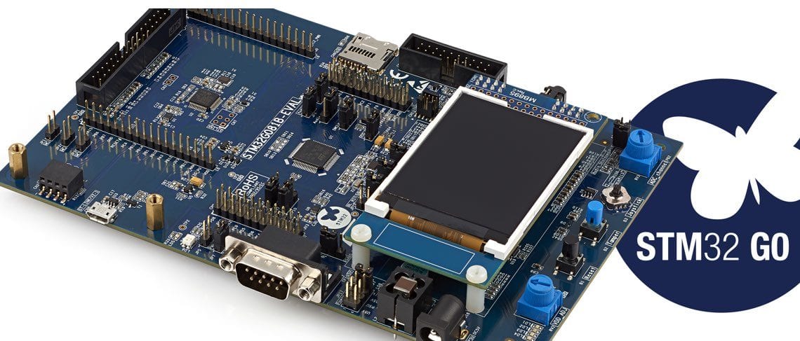
We named our new series STM32G0 because it builds on the foundations of the STM32F0. However, instead of using its 180 nm process node, it relies on a 90 nm node similar to the STM32L4. Using this new lithographic method enabled us to benefit from some of the ultra-low-power capabilities of the L4, while also integrating more components and optimizing the architecture to push the performance and features of the F0 to an entirely new level. Hence, the STM32G0 ensures that engineers can find the right balance between computationally intensive functionalities and the system’s power draw. And to enable them to test this new paradigm as soon as possible, we are releasing STM32G0 Nucleo boards and EVAL boards, which will allow them to see how they can easily port their applications and right away enjoy the increase in I/Os and memory.
Nine More I/Os and One Single Power Line

All the benefits of the new architecture may not always be evident to everyone, but the increase in I/Os is particularly essential. For instance, the 64-pin version of the new STM32G071 offers nine more I/Os than the STM32F071 that has a similar pin count while the 48-pin model provides seven additional I/Os compared to the STM32F071 that uses the same package. We are also going one step further by launching an STM32G071 with 32 pins to offer even more flexibility. Indeed, there was never an STM32F071 with only 32 pins, but if we look at the next best thing, the STM32F051 has less memory, less RAM, and five fewer I/Os. Hence, developers that wanted a 32 pin version of the previous generation STM32F071 or more I/Os can now enjoy a whole new range of possibilities.
The new STM32G0 also does a lot to simplify PCB design, but one feature stands out: the single power supply pair on packages that have 64 pins or fewer. Instead of having the traditional multiple power lines and their necessary capacitors, the STM32G0 uses only one line, which will make the PCB design a lot simpler and cheaper. To achieve such a feat, we developed a patented internal bonding system within the package that is able to propagate current to all the various units of the architecture to power analog and digital circuits.
The Poster Child of Customizable MCUs

The STM32G0 is also special because our willingness to offer an extensive array of packages gives new meaning to the simplicity and robustness of our architecture. Indeed, today’s announcement is highly symbolic because we are not just launching a handful of part numbers, but committing to releasing one of the most comprehensive families of products.
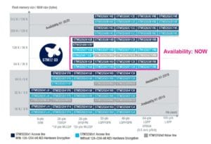
We are envisioning a wide array of packages: some with as little as 8 pins and others as high as 100 pins. Moreover, our 32 pins and 48 pins models go from the simplest configuration with 8 KB of RAM and 16 KB of Flash to our most powerful 128 KB RAM / 512 KB Flash architecture. This tremendous variety ensures engineers can choose the part that is most relevant to them. For example, teams no longer need to switch to an STM32F1 to benefit from 512 KB of Flash but can enjoy the low power consumption of the STM32G0 while still benefitting from half a megabyte of storage.
Additionally, this large selection of models within a package addresses a new trend called “customizable MCU.” Currently, wearables and mobile devices offer one microcontroller per product. However, manufacturers are looking into providing multiple versions of a product, each using a different MCU, to create a pricing structure that can catch more customers. Those looking for entry-level models will be glad to have a more cost-effective solution with less memory, while people willing to invest in more performance will also have the possibility to do so, and the manufacturer will end up appealing to a broader audience. Thanks to our new STM32G0 series, designers benefit from a wide range of configurations that all use an identical package, thus enabling them to keep the same PCB and code while offering various MCU options.
A Hybrid Between Ultra Low Power and Mainstream Performance
Another aspect of the new architecture that will facilitate application programming is the low power modes of the new component. Despite being a mainstream device, the STM32G0 requires less than 100 µA / MHz when running at 64 MHz, thanks to its process node that has some similarities with the STM32L4. Comparatively, the STM32F0 requires 250 µA / MHz. The new architecture also has a STOP mode that can go as low as 3 µA with only the Flash and Real-Time Clock off, while its STANDBY mode just demands 200 nA, which is drastically less than anything on the previous generation. Despite such a low power state, the architecture can still wake up in about 5 µs in STOP and 14 µs in STANDBY, making them even more advantageous.
Additionally, we also offer a VBAT pin, which means that engineers can put a capacitor to only power the RTC and backup registers, which allows the rest of the system to shut down and drops the power consumption to 10 nA. With such a low consumption, it is possible to create a design that keeps basic information in memory while the user replaces a battery, for instance, thus improving the overall experience. Writing an application is often about finding the best optimizations, which can take a lot of time and effort. Hence, since the power consumption of the STM32G0 is so low, its power-saving features open the way for new applications and levels of performances. It is thus possible for engineers to treat it as a form of hybrid that’s almost an ultra-low device while remaining a mainstream MCU.
An STM32G0 for Security

To prepare teams for the next generation of IoT products, we included a crypto-core capable of accelerating AES 256 bit computations, as well as a true random number generator to optimize cryptographic keys. However, the most impressive security feature is the implementation of a programmable securable memory area. Developers can define a portion of the Flash that will be inaccessible from the rest of the system once they log out of it, which enables them to store root keys and critical routines to implement features such as Secure Boot and Secure Firmware Upgrade. We know that many teams will thus use the extra memory of the STM32G0 to implement the Securable Memory Area to protect their application, thus increasing their product security without compromising performance.
Moreover, for the first time ever, one of our budget mainstream MCU includes a Memory Protection Unit (MPU). It guards against attacks that attempt to duplicate data or eavesdrop by creating a sandbox that isolates program threads while also supporting secure Operating Systems. The feature stood out when we delved into an STM32L4 Discovery Board, and after being completely absent on the STM32F0, its presence on the STM32G0 marks a new and highly symbolic step in our desire to bring critical security features to all products. Additionally, to help customers even further, we will provide technical documentation, software reference package, and security guides in the coming months, to assess developers as they take advantage of these features.
An STM32G0 For Innovation
STM32G0 is also the world first general purpose ARM Cortex-M microcontroller to support USB-C and Power Delivery (UCPD) thanks to two UCPD interfaces. This new IP enables the management of a Type-C connector without requiring an external Power Delivery controller. We also included a transceiver to handle the Power Delivery communication protocol for applications that need more power (up to 100W) or for those that wish to use alternate modes to deploy authentication, firmware upgrade, or video sharing over USB-Type-C, for instance.
Similarly, we also integrated the same high-speed and highly accurate internal clock as the STM32L4 to simplify the PCB design even further. We also have timers that can run twice as fast as the MCU (up to 128 MHz) to offer much higher control over digital systems. For instance, smart light makers can enjoy a lot more precision and vastly reduce flickering effects on some of their models.
Future-Proofing To Make It Last Longer
Ultimately, it’s all part of our efforts to future-proof our new architecture, which explains why we also included a faster Analog-to-Digital Converter (ADC) with a 16-bit precision through hardware oversampling. Additionally, our new device is a lot more robust thanks to new components that make the overall design a vastly less susceptible to electromagnetic interferences and offer a much better protection against fast transient voltage. For instance, the STM32G0 can tolerate bursts higher than 4.5 kV on the pins and 8 kV on the board. And to help developers prepare for the future, we are announcing updates to STM32CubeMX within this month as well as a new STM32CubeMonitorUCPD utility that will be available around Q1, 2019 and that specifically targets USB-C and Power Delivery devices.


