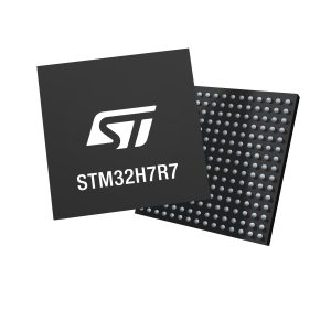
The STM32H7R and STM32H7S are the fastest STM32 MCUs at 600 MHz and the most cost-effective STM32H7s, thanks to their smaller flash memory. They target integrators who must use external storage and will, therefore, be able to lower their bill of materials by choosing an MCU better tailored to their needs. Additionally, while there’s less flash, the STM32H7R and STM32H7S are the first to support bootflash instead of the traditional boot ROM. Some also offer a NeoChrom GPU. Consequently, as consumers demand that embedded systems get better graphics, thus forcing designers to rethink their hardware configuration, the STM32H7S and STM32H7R are making rich and modern UIs far more accessible.
Offering more design freedom

It’s increasingly challenging to find the MCU that perfectly suits an application. Too often, engineers face an edge case or are working on a system with unique constraints. Consequently, they must usually settle for an MCU that doesn’t always meet their requirements. A device may have too much or too little memory, computational power, peripherals, etc. The problem is even more significant when dealing with cost-constrained BoMs, which are common in embedded systems. In many instances, a few dollars can make a huge difference. That’s why the STM32H7R and STM32H7S aim to be as close to a bespoke solution as possible.
STM32H7R3/S3 vs. STM32H7R7/S7
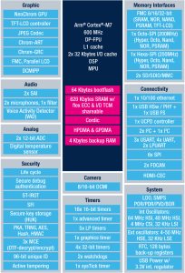
To help engineers optimize their configuration, ST is launching two types of devices. The general-purpose line, the STM32H7R3/S3, features a Chrom-ART accelerator for 2D graphics. It has already helped optimize numerous graphical user interfaces by fetching assets from memory faster and accelerating operations like 2D copies, transparencies, or alpha-blending. Overall, these computations would take about twice as long, in some cases, if handled by the CPU. Consequently, Chrom-ART has enabled modern UIs on even the most constrained devices like smartwatches and wearables. The STM32H7R3/S3 thus open the door to a lower bill of materials for projects that need to optimize a traditional 2D GUI.

On the other hand, the STM32H7R7/S7 provides the NeoChrom GPU inaugurated on the STM32U599. The hardware IP is a 2.5D accelerator optimizing texture mapping with bilinear and point sampling, among other things. Consequently, it accelerates animations and drawing operations, thus offloading the Cortex-M7 by up to 90%. Furthermore, Neochrom GPU has an 8-bit Octal Serial Peripheral Interface (OSPI) or a 16-bit high-speed interface (HSPI) to fetch assets from the external memory modules faster and deliver them to the L2 cache.
STM32H7R vs. STM32H7S
The only difference between the STM32H7R and STM32H7S is that the latter focuses on security. The STM32H7S can decrypt and encrypt information from the RAM on the fly, making it the first STM32H7 to do all this. Previously, some STM32H7 devices had on-the-fly decryption (OTFDec), which enabled developers to use secure code without a performance penalty. Now, thanks to on-the-fly encryption (OTFEnc), the STM32H7S can protect user data from intruders, among other things. It is also ST’s first MCU to offer a special encryption mechanism to external flash and RAM modules. These features, as well as other physical protections, mean the STM32H7S is the first STM32H7 to target SESIP Level 3 and PSA Level 3 certifications.
10 packages
Thanks to our mastery of the lithographic operations behind the STM32H7, we released ten packages for each general-purpose line (from 68 pins to 225 pins) and five for devices with a NeoChrom GPU (from 144 pins to 225 pins). Early adopters of the STM32H7 can now run vastly more complex UIs with minimal effort since their code and PCB layout will easily port to the new STM32H7R and STM32H7S.

Greater performance on an MCU
More power and peripherals
Every STM32H7R and STM32H7S has a Cortex-M7 core running at 600 MHz. There are also serial and parallel memory interfaces offering to optimize communication between the MCU and the external memory modules. The new STM32H7S and STM32H7R also enjoy, for the first time on an STM32H7, a new high-speed USB PHY, and a USB Power Delivery controller. They are also the first STM32H7s to get an I3C interface. Put simply, the device allows developers to have a UI at an HD resolution and still run a machine learning or communication application at the same time.
Bootflash
The STM32H7R and STM32H7S have 64 KB of embedded flash. Unlike some competitors that remove the flash, we know that embedded memory can help with performance, even if the application heavily relies on external memory. We thus settled on 64 KB because it brings a real cost advantage while facilitating the management of field firmware updates or feature releases. Moreover, unlike traditional MCUs that use a ROM for their bootloader, the entire flash of the STM32H7R and STM32H7S can house the boot sequence, making it much more flexible and valuable. We also updated STM32CubeMX, which will help configure the bootflash and manage external memory modules for greater simplicity.


