ST recently launched a WLCSP36 version of the BlueNRG-LPS, thus shrinking the SoC to a package that measures 2.652 mm x 2.592 mm. It also widens the portfolio we created more than a year ago when we released the QFN32 version by enabling engineers greater packaging options. Engineers benefit from an identical radio and MCU (Cortex-M0+), meaning they can choose a BlueNRG based on their memory needs (256 KB of flash and 64 KB of RAM for the BlueNRG-LP versus 192 KB and 24 KB for the BlueNRG-LPS) and application purposes.
Indeed, the BlueNRG-LP and BlueNRG-LPS were the first BLE SoCs to support up to 128 concurrent connections. Both handle long-range, 2 Mbps transfers, advertising extensions, +8 dBm output power, and the broadest dynamic range ever on an ST Bluetooth chip, to name a few. The BlueNRG-LPS distinguishes itself by its ability to figure out the direction of a Bluetooth signal with the angle of arrival (AoA) or angle of departure (AoD) methods. Both use an array of antennas and geometry to enable more accurate location tracking. As for the BlueNRG-LP, it supports two I2C and two SPI interfaces instead of one for each on the BlueNRG-LPS to tackle more demanding data processing requirements.
Understanding New Industrial and Technological Challenges
When choosing a Bluetooth SoC, engineers study, among other things, the most recent trends shaping their industry. Industrial applications must connect even more sensor nodes to a gateway. Bluetooth SoCs must also offer more processing power while keeping bills of materials low and power consumption down. Meeting these challenges demands optimizations at the radio and microcontroller levels. Merely connecting up to 128 devices at a time is not enough. Engineers will ask two critical questions: “How good are these connections?” And “What can I do with them?” The answers lie in how the BlueNRG-LP and BlueNRG-LPS provide more performance, better security, greater efficiency, and lower costs.
BlueNRG-LP and BlueNRG-LPS: More power, more security, and more energy efficiency
High-speed
Teams working on industrial applications must deal with significant constraints that influence both range and data rates. For instance, a gateway connecting to many boards throughout a smart factory must cover incredibly long distances and support a robust data rate for firmware updates. The ST SoCs achieve both. By offering an LE 2M PHY, the BlueNRG-LP and BlueNRG-LPS can reach data rates of up to 2 Mbps. Comparatively, the LE 1M PHY in previous BlueNRG SoCs stopped at 1 Mbps. The faster transfers are possible thanks, in part, to the larger payloads from Data Length Extension, as we explained in our BlueNRG-2N blog post, and bandwidth increases inherent to Bluetooth 5.0.
Long-range
BlueNRG-LP and BlueNRG-LPS also offer greater coverage. Unfortunately, many engineers overlook this long-range functionality because they underestimate its potential. The ST SoCs offer LE Coded PHY, enabling far greater distances between two Bluetooth devices without requiring an additional power amplifier. ST’s real-world tests, which used existing development boards and applications, reached 1.3 kilometers (0.8 miles) when there were no obstacles between the transmitter and receiver.
The increase in range is possible because LE Coded PHY uses, among other things, Forward Error Correction, which adds additional bits to each packet. However, data redundancy leads to a lower bandwidth of 125 kbps. Another feature that helps avoid interferences is Channel Selection Algorithm #2 (CSA #2). While CSA #1 could only hop between 37 channels, CSA #2 has 65,535 channels at its disposal. This extensive selection helps avoid collisions and fading effects. Whether there are a lot of devices nearby or great distances between them, CSA #2 increases the network’s reliability. The longer range is also possible because the devices better handle the background noises that inevitably plague a signal when covering great distances.
Link budget
Engineers working on Bluetooth applications always run a link budget analysis, a design aid that helps them anticipate overall performance. Put simply, it ensures designers can foresee specific issues, such as an insufficient signal strength incapable of reaching the receiver. In most textbooks, a link budget analysis uses the following equation:
Received power (dB) = transmitted power (dB) + gains (dB) − losses (dB).
However, engineers work today with data sheets that almost always give the transmit power (TX) and receiver’s sensitivity level (RX). Hence, most real-world projects define their link budget according to the following equation:
| Link Budget (dB) | = TX Power (dBm) – Sensitivity level (dBm).
The BlueNRG-LP and BlueNRG-LPS have a TX power capable of reaching +8 dBm (programmable in 1 dBm steps) and an RX sensitivity of -104 dBm at 125 kbps or -97 dBm at 1 Mbps. Hence with a link budget of 112 dB and 105 dB, the ST SoCs have one of the most significant link budgets in the industry. As a result, engineers can anticipate better performances at identical power consumption compared to devices with a lower link budget.
Thwarting hackers
Security is another crucial aspect that engineers focus on when designing a system. Consumers are a lot more sensitive to issues of privacy and data protection. As a result, teams must implement features that shield users. BlueNRG-LP and BlueNRG-LPS provide answers to these critical engineering challenges. One of them is the presence of a secure boot loader that checks the firmware’s signature before launching it. Such measure protects against rootkits or low-level attacks. To protect the flash, developers can also disable SWD and UART access. Similarly, 1 KB of memory is one-time-programmable to guarantee its integrity. Hence, theoretically, a hacker with access to the device wouldn’t be able to clone or modify its content.
More Computational Throughput and a Lower Power Consumption
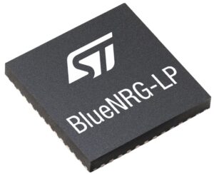
Developers must find ways to improve performance, accuracy, and user experience. Engineers often turn to a device with more computational throughput to solve this challenge. However, many Bluetooth end products must have a low power consumption to preserve battery life. Engineers ought, therefore, to find a way to reconcile these seemingly contradictory requirements.
BlueNRG-LP and BlueNRG-LPS answer this challenge with their Cortex-M0+ running at 64 MHz. Moreover, ST also provides a free-of-charge Bluetooth-SIG certified Mesh stack (STSW-BNRGLP-Mesh). As a result, it becomes very easy to cover large areas and reach up to 126 hops or 32,000 nodes. Yet, despite all this, the SoCs feature a low power consumption of 4.3 mA (peak current in transmission at 0 dBm). Similarly, the devices peak at 3.4 mA in RX (at sensitivity level) and only need 0.64 µA in DEEPSTOP mode with full RAM retention.
BlueNRG-LP and BlueNRG-LPS: More cost-effective designs
Lowering the bill of materials
Some engineers put a lot of weight on overall costs. The SoCs must thus offer unique advantages that reduce the bill of materials. ST components address this problem by integrating a 12-bit analog-to-digital converter (or 16-bit with a decimation filter) with eight input channels. The increase in precision from previous SoCs means they can now have a programmable gain amplifier. The PGA amplifies an audio signal from 0 dB to 30 dB, thus allowing the use of analog microphones. Compared to digital microphones, analog alternatives are more cost-effective, thus ensuring a lower bill of materials.
Another pathway to a more cost-effective system is through the use of fewer external devices. Hence, we designed the BlueNRG-LP and BlueNRG-LPS to embed more components and simplify PCBs. For instance, the SoCs now have six load capacitors. Consequently, designers can use a high-speed crystal without soldering external capacitors onto the PCB or, in some instances, entirely abstain from using a 32 KHz crystal because the embedded low speed internal (LSI) is precise enough to act as a clock source.
The ST devices also integrate the RF balun, meaning engineers no longer need dedicated ones. The components also have only one RF single-ended output pin, simplifying the layout. And to make things even easier, we also provide matching filters, such as the MLPF-NRG-01D3. Engineers don’t have to worry about matching the impedance to get the most out of the Bluetooth SoC, thus vastly accelerating prototyping. Finally, the SMPS of the BlueNRG-LP and BlueNRG-LPS have a higher clock. As a result, designers can use a smaller and more cost-effective inductor.
An extensive price structure
A low unit price is critical as engineers search for a Bluetooth SoC and justify their choice to their hierarchy. ST provides various memory configurations to meet this challenge and keep the Bluetooth SoCs cost-effective. Since the Bluetooth stack typically takes 80 KB to 100 KB, developers get between 100 KB and 150 KB for their application, which is often enough. If designs need significantly more storage, much more powerful computational capabilities, or ad-hoc peripherals, they will naturally gravitate toward the BlueNRG-2N and a dedicated host MCU.
We further optimized our pricing structure by offering four types of packages. The QFN32 and WLCSP36 have 20 GPIOs, while the QFN48 and the WLCSP49 have 32 and 26, respectively. Put simply, teams needing smaller flash and RAM or fewer pins don’t need to pay more. Similarly, we offer models that can go up to 85 ºC and identical ones that can reach 105 ºC. Industrial designs will gladly use the latter, while others will choose the former and save.
BlueNRG-LP and BlueNRG-LPS: Getting started
STEVAL-IDB011V1, STEVAL-IDB012V1, and STEVAL-IDB013V1 evaluation boards
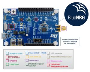
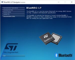
The process engineering teams undergo to select a Bluetooth SoC is often complex. Many factors may influence a decision, from costs to past experiences, performance, and ease of use. Hence, to help teams evaluate the BlueNRG-LP and BlueNRG-LPS faster, we often release updates to our software and development tools. For example, programmers can use the STEVAL-IDB011V1 BlueNRG-LP or the STEVAL-IDB012V1 and STEVAL-IDB013V1 BlueNRG-LPS evaluation boards with the BlueNRG Navigator GUI to hasten development operations. The software can upload example applications, thus helping managers see what to expect from our SoCs.
BlueNRG Developer Kit and BlueNRG GUI
The BlueNRG Developer Kit offers a Navigator, a graphical user interface enabling developers to access demo applications and their source files quickly. For instance, we include a sample beacon program, a remote control, a sensor profile demo, and various security feature implementations. Developers can even experiment with the Secure Bootloader GUI tailored for the BlueNRG-LP and BlueNRG-LPS. Once engineers are ready to move to their application, the BlueNRG GUI will assist them in configuring their Bluetooth LE SoC. The tool offers a visual representation of command packet tables and register values, among other things, thus simplifying developments.
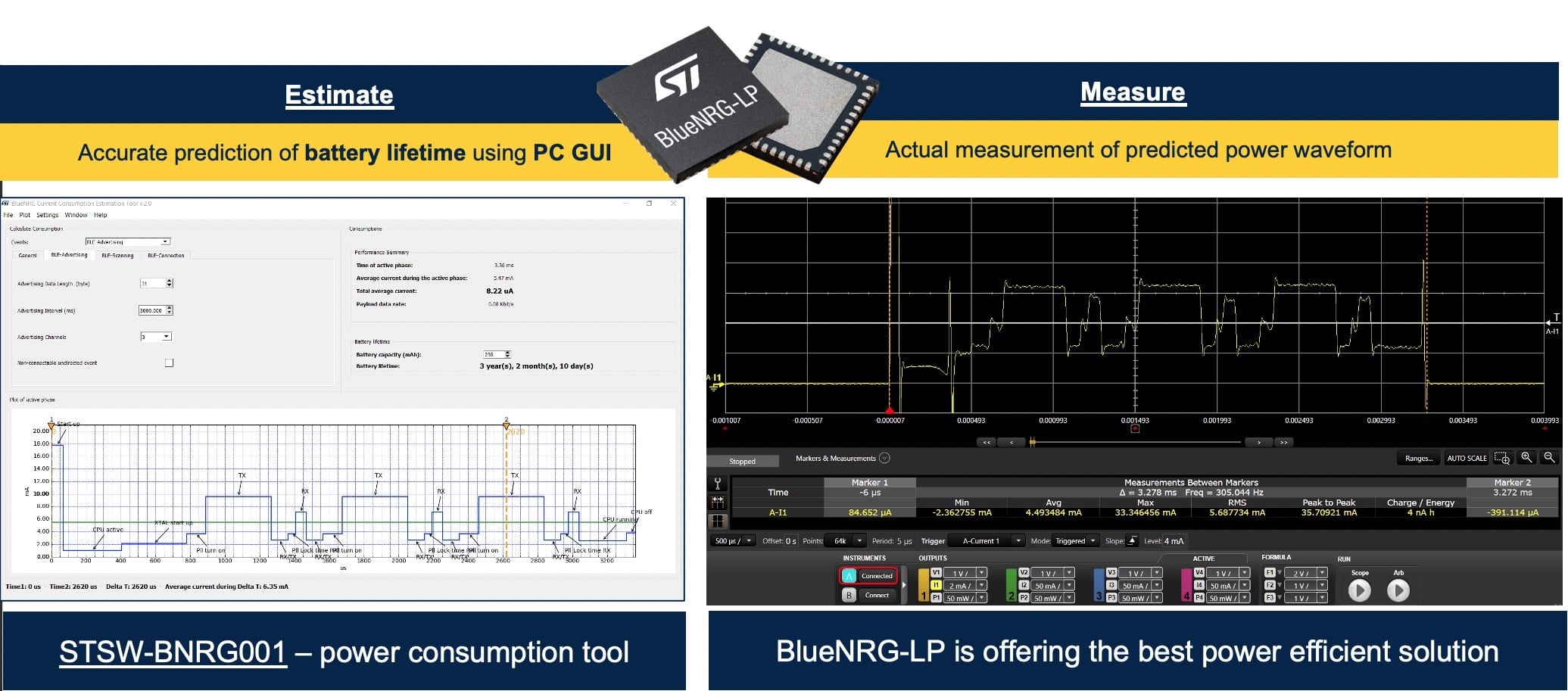
ST also provides the BlueNRG current consumption tool. The utility offers a graphical representation of the low-power capabilities of our Bluetooth SoCs to help engineers and decision-makers visualize real-world power consumption measurements. For instance, the software displays average estimates, battery life, and data rates. Consequently, it’s easy to see how various use cases affect the overall power consumption. Developers may also easily move from the BlueNRG-LP to the BlueNRG-LPS and vice versa since both use a Cortex-M0+ and share compatible peripheral drivers and Bluetooth stacks.
