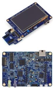
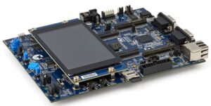
Check out our new videos describing how to get started with our Discovery boards for the STM32H747 (dual-core) and STM32H750 (Value Line)
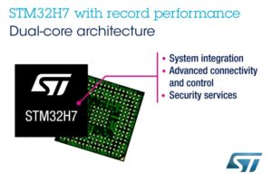
ST is releasing today new STM32H7 microcontrollers to make this series of MCU more powerful, flexible, and accessible. The STM32H745/STM32H755 and STM32H747/STM32H757 are ST’s first dual-core models with a Cortex-M7 running at 480 MHz and a Cortex-M4 at 240 MHz, thus reaching 3220 points in CoreMark. On the other end of the spectrum, we are also officially releasing the STM32H742 and STM32H750, both of which get the same Cortex-M7 at 480 MHz but offer cost-effective architectures to make the H7 line even more affordable. It is thus a highly symbolic announcement as it broadens this series of MCUs to make it relevant to more designs and guarantee that more customers find the performance, feature, and price point that’s pertinent for their application.
In 2016, the STM32H7 became the most powerful Cortex-M7 on the market and broke the 2000-point threshold in CoreMark. During the following years, our foundries continued to work on optimizing their manufacturing processes to increase performance and tailor the architecture to various industry demands. For instance, the new STM32H742 removes the TFT LCD controller and the JPEG Codec unit while also dropping the RAM to 692 kB to ensure that systems that don’t need a display find in it a better value proposition. Similarly, we announced last year the creation of an STM32H7 Value Line with a lot less Flash so designers that require external QuadSPI for graphic-intensive applications don’t have to pay for embedded storage they will never use. Today, the STM32H750 is the first Value Line MCU commercially available in the STM32H7 series.
Let’s explore the other benefits that we were able to bring to the STM32H7 by improving our manufacturing processes.
The Most Powerful New Feature of the STM32H7 Series: An Additional Cortex-M4

The most obvious performance boost comes from the addition of a Cortex-M4 core which increases the CoreMark score by 800 points. However, it’s very easy to miss the fact that beyond the simple addition of a processing unit, it is its implementation into the die that makes the STM32H745/STM32H755 and STM32H747/STM32H757 truly special. Thanks to a masterful design, this dual-core architecture is highly flexible. For instance, the system can boot on either core, and they each exist in an independent power domain to optimize energy consumption significantly. For example, when an application doesn’t require the Cortex-M7, developers can turn its power domain off without any impact on the other core. As a result, the new dual-core models have a dynamic power consumption far better to that of the STM32F7.
The flexibility also translates into a more straightforward development phase. Taking advantage of multiple cores can seem daunting, but companies that already wrote applications for our Cortex-M7 or Cortex-M4 STM32s can reuse some of their code and build upon it. For instance, a company using an STM32 Cortex-M4 to control an industrial pump can take its existing application then run a new display and a graphical user interface on the Cortex-M7 to add new features to their products without rewriting everything. Very simply, engineers get the benefits of two MCU without the complexities and design challenges that would come from having two different components on the PCB.
New Features in the Dual Core STM32H7: MIPI-DSI, 16-bit ADC, and FD-CAN
The improvements to our lithographic operations also enabled us to bring a MIPI display serial interface (MIPI-DSI) for the first time in an STM32H7. The feature, present in the STM23H7x7, allows the use of higher-resolution displays and offers low electromagnetic interferences while requiring little power, which makes it an excellent fit for portable video game consoles or appliances, among others. Similarly, the new STM32H7x5 and STM32Hx7 enable a more flexible use of the three 16-bit analog-to-digital converters (up to 3.6 Mega Samples per second) present on the die. Its two FD-CAN interfaces and its Ethernet controller also offer an excellent advantage for industrial applications.
New Features in All the New STM32H7: Dual-Bank Flash, and Root Security Services

The optimizations to our processes also yielded new features that are available on all the new STM32H7 and the existing STM32H7x3 which use a different revision since April. Our data sheet refers to it as “Rev V” and its Finish Good number finishes with a “7” (i.e., 32H743IIT6$Y7). Among other things, the new revision brings dual-bank Flash, except to the STM32H750 as it relies on 128 kB of embedded Flash and external Flash anyway. Dual Bank Flash divides the storage capacity into two parts, uses the first part for the application, but can load new firmware in the second before performing a hot swap to run the system on the latter without any interruption, enabling major updates without any downtime.
Another feature is the Root Security Services (RSS), present on the STM32H7s with a crypto core (i.e., STM32H75x), including the STM32H753 Rev V. Taking the form of a boot loader, engineers can use it to securely install a firmware. Since the MCU stores an encryption key, companies can ship an encrypted firmware to an assembly line responsible for installing it and the decryption operations will only take place within the MCU to protect IPs and prevent hacking. Additionally, we also offer a “counter protection”, meaning that developers can define the number of MCUs that will receive the firmware and the component will halt its installation operations if the system reached the upper limit. It allows engineers to know if someone installed their firmware on a component that doesn’t belong in their inventory and can thus prevent leaks into the gray market.
Optimizations in All the STM32H7: Higher Ambient Temperature
Improving our foundries’ operations also enabled us to bring essential optimizations to the current STM32H7 architecture, such as the ambient temperature at maximum power dissipation (TJmax 125 ºC). If the upper threshold for previous models was at 85 ºC, the new STM32H7s can now safely reach 105 ºC. Furthermore, to ensure that all the variants of the STM32H7 benefit from this revision, the STM32H7x3 Rev V MCUs will also be able to run at this new ambient temperature. Going from 85 ºC to 105 ºC means being able to run specific applications without active heat dissipation, thus benefiting from the silence of heat spreaders instead. It also opens products to a wider range of environments.
Moreover, the dual-core versions of the STM32H7 include a switched-mode power supply (SMPS) to improve the MCU’s power efficiency significantly compared to a microcontroller using a more traditional LDO. The gain is so drastic that if engineers use the SMPS, they can increase the maximum junction temperature up to 140 ºC with a cap on the frequency at 300 MHz, which is a lot more practical than competing products that may sometime advertise higher temperatures but require much lower frequencies. It’s also a testimony that unlike traditional designs that struggle with power efficiency as they add more processing cores, our new architecture bucks common trends to offer better power consumption, even after the addition of a whole new core.
Grab a Board and Get Started

The best way to start experimenting our STM32H7x7 dual-core MCUs is to get the STM32H747I-EVAL or the STM32H747I-DISCO boards. The latter integrates a 4″ MIPI-DSI touchscreen to facilitate the development of a graphical user interface, and in a few months, both of these boards will have an alternative version embarking a crypto core (i.e., STM32H757I-EVAL and STM32H757I-DISCO). Similarly, engineers who are interested in the STM32H750 Value Line can grab an STM32H750B-DK Discovery board, which will have a 4.3″ TFT display and will come with TouchGFX demos. They may also get one of the many Nucleo board that will feature one of these new components.
- Learn more about the STM32H7x5 and STM32H7x7
- Check out the STM32H750
- Discover the STM32H742
