Update, March 2, 2021
ST recently held an updated version of its webinar on the MasterGaN family and we are now making it available on demand. Anyone who missed it, or those who wish to rewatch it, can thus get a copy by simply submitting their email. The session begins with an overview of power conversion trends followed by an introduction of the MasterGaN platform, which includes MasterGaN1 through MasterGaN5 devices. After providing a high-level understanding of the product and its technology, the presentation explores specific circuit topologies. We also used the EVLMG1-250LLC to show how to use a MasterGaN1 in a compact and highly efficient DC/DC resonant converter for industrial applications.
• Watch the webinar now to improve your knowledge of GaN solutions
Original text, September 30, 2020
To improve the accessibility of our content, please find the audio version of this blog post.
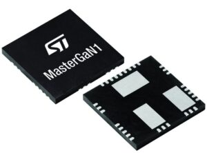
We are launching today the MASTERGAN1, the first and only 600 V single package to include a gate driver and two Enhancement mode Gallium Nitride (GaN) transistors. Similar competing devices only offer one GaN. However, ST decided to double that to enable a half-bridge configuration and allow the MASTERGAN1 in new topologies. For instance, engineers can use it in LLC resonant converters when designing a AC-DC system. The device will also fit other common high-efficiency and high-end topologies, like active clamp flyback or forward. It also addresses higher power ratings and totem-pole PFC.
The new device is highly symbolic because it makes it easier to use GaN transistors in more common products. When the industry first used these power devices, it was in telecommunication equipment or power supplies for data centers. Thanks to MASTERGAN1, engineers can now envision much more efficient power supplies for ultra-fast smartphone chargers and USB-PD adapters, among many other things.
Why Gallium Nitride in a Power Supply for Smartphones?
Many consumers are oblivious to it, but the power from smartphones, tablets, or laptops chargers increased exponentially in recent years. Manufacturers face a difficult problem. Battery capacity remains mostly the same, due in part to a lack of breakthroughs in material design. Hence, instead of offering bigger batteries, mobile devices simply charge faster. Thanks to USB Power Delivery (USB-PD) and fast charging technologies, it’s possible to reach 50% in less than ten minutes. This is only possible because chargers are now able to output as much as 100 W in some cases. However, to keep the overall dimensions close to what we have today, the system needs high switching frequencies.
If chargers with GaN transistors aren’t yet on every corner, it’s because designing them was a significant challenge. Take the average engineer in a medium or even a large company. That person would first encounter a simple cultural challenge. Convincing managers and executives isn’t always easy. Nevertheless, it is essential to help decision-makers understand the technology. Once the engineer’s project received all the necessary approvals, designing the PCB is far from simple. It’s easy to create an underwhelming PCB. Moreover, implementing proper safety measures is paramount. The significance of the MASTERGAN1 resides in its ability to solve all these issues and popularize GaN in a lot more applications.
MASTERGAN1: Understanding Gallium Nitride
GaN Electrical Properties

Gallium Nitride shines when requiring high power in a small device because of its inherent properties. The material itself is nothing new. We use it since the 90s in LEDs and since the 2000s as the blue lasers in Blu-ray readers. However, founders are now able to grow a thin layer of GaN on a silicon wafer to create transistors with unique properties. GaN has a bandgap of 3.39 eV, which is far higher than silicon (1.1 eV) and Silicon Carbide (2.86 eV). As a result, its critical electric field is also much higher, which means it offers far greater efficiency at high frequencies.
The high bandgap at the root of these properties comes from the molecular structure of GaN. Gallium, by itself, is a very poor electrical conductor. However, when nitrogen atoms disrupt the gallium lattice, it significantly increases the structure’s electron mobility (1,700 cm2/Vs). Electrons can thus move at a greater rate with fewer losses. As a result, applications that require a switching frequency above 200 kHz are much more efficient with GaN. It enables smaller and more cost-effective systems.
Seeing the EVALMASTERGAN1 Is Believing
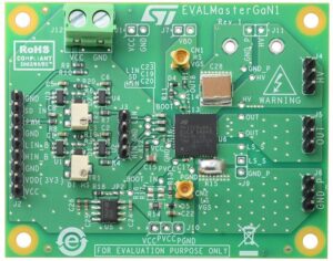
Despite all this theoretical knowledge, it may still be difficult to convince decision-makers. After all, GaN transistors are not new, but their use in the power supply of high-volume products is still a novelty. Showcasing the capabilities of GaN and the MASTERGAN1 becomes vastly more straightforward thanks to the EVALMASTERGAN1 board. Showing a physical platform makes it real and what the single package in a power supply would look like. It is even possible to customize the board. One can add a low-side shunt or an external bootstrap diode, among other things, to better resemble the final design. It also becomes easier to showcase its support for a vast range of supply voltages. Additionally, all pins of the MASTERGAN1 are accessible to help developers test their applications early.
MASTERGAN1: Designing With Gallium Nitride
Reducing Design Complexities

Going from a proof-of-concept to a custom design can be challenging. The schematics of the evaluation board are a great starting point, but high-frequency applications are tricky. Induction parasitic can cause issues if the traces on the PCB are too long. It is also important to include two GaN transistors for a half-bridge converter, but most of the competing devices only offer one. The MASTERGAN1 is thus a unique product because it is today the only single chip that integrates two GaN transistors. As a result, engineers don’t have to deal with the complexities associated with these types of applications. Similarly, the particular GaN technology and optimizations at the gate driver, means the system doesn’t require a negative voltage supply. MASTERGAN1 also has input pins compatible with 20 V signals. Engineers can thus use it with a wide range of existing and upcoming controllers.
Engineers must also deal with critical size constraints. A smartphone charger must remain small. The fact that the MASTERGAN1 package measures only 9 mm x 9 mm is thus a considerable benefit. Additionally, as we scale this new series with new devices in the coming months, we’ll keep them pin-to-pin compatible. Hence, using another member of the MASTERGAN family will be more straightforward. Creating a new design based on a PCB that uses the MASTERGAN1 will be simpler. Finally, being able to design a smaller PCB quicker represents a substantial cost-saving. As manufacturers battle to make a more affordable solution, the MASTERGAN1 helps make designs more affordable. It also explains why we already have design wins.
Increasing Robustness
Another major challenge for engineers lies in creating a robust design. Exploding chargers end up overall social media. Unreliable systems constitute a significant strain on customer service operations. But implementing safety features is far from easy. When dealing with GaN half-bridge topologies it is imperative to avoid turning both on simultaneously. The MASTERGAN1 thus integrates an interlocking function, matched propagation delays, and differentiated turn-on and turn-off gate currents. Such features enable clean and efficient switching. Finally, we designed the gate driver of MASTERGAN1 for e-MODE GaN FETs, thus boosting both performance and ruggedness.
The under-voltage lockout (UVLO) protection, optimized for GaN FETs, prevents the considerable loss of efficiency and potential issues. Such problems may come from operating at low supply voltage. Similarly, the integrated thermal shutdown protects the device from overheating. The gate driver’s level shifters and effective input buffering make the GaN’s gate driving very robust and noise immune. Finally, the shutdown pin allow a dedicated line from the MCU to set the device in idle mode.
