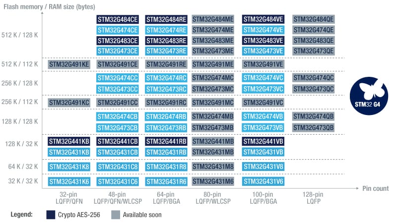
The STM32G4 microcontroller series is the first ever to include five analog-to-digital converters, seven digital-to-analog converters, six operational amplifiers, and seven comparators, while also integrating a USB-C Power Delivery controller, a 184 picoseconds high-resolution timer, CAN interfaces with flexible data rate, and math units accelerating certain trigonometric functions. Near the STM32F4 when it comes to computational throughput, the STM32G4 remains alone in the “mixed-signal” MCU segment by offering new and optimized features for both digital and analog applications. Its Cortex-M4 will reach up to 170 MHz to obtain 213 DMIPS, and 550 points in CoreMark while its numerous architectural improvements enable the creation of simpler yet more robust designs. We are also using two different dies at launch to offer the broadest range of pins and memory configurations possible right from the start.

This new architecture draws from the general-purpose DNA of the STM32F3, but also adds innovations and optimizations to answer the peculiar needs of various markets. For instance, the math accelerators make it an excellent MCU for field-oriented control (FOC) computations or digital power supplies while its CAN FD support will benefit industrial products. By integrating more analog and digital components on its die, the STM32G4 enables the creation of denser and more powerful power supplies for server farms and more cost-effective consumer products. Moreover, it is a way to future-proof designs. For example, the rise of silicon carbide (SiC) devices in cars or gallium nitride (GaN) transistors demand more precise timers to adapt to their higher switching frequencies. Thanks to its 12-channel high-resolution timer, the STM32G4 is already capable of driving the designs that will rest on these components to shape the electronics of tomorrow.
The Innovations of the STM32G4
The New Math Accelerators

The STM32G4 is the first STM32 with two math accelerators, one for trigonometric calculations (COordinate Rotation DIgital Computer or CORDIC) and the other for filtering functions (Filter Mathematical ACcelerator or FMAC). Very simply, the CORDIC accelerator provides hardware acceleration for the trigonometric functions often present in motor control, metering, signal processing, and many other applications. On the other hand, the FMAC enables the implementation of two major primary filters in signal processing: the finite impulse response (FIR) and infinite impulse response (IIR) digital filters.
In a brushless DC motor (BLDC/PMSM), currents at the phases create a reference frame of the stator in a two-coordinate system (alpha axis and beta axis). FOC then computes vectorial changes to accurately control the motor’s rotation, which explains why the ability to solve trigonometric functions in hardware significantly increases performances. Similarly, engineers can feed a time domain to the IIR and FIR filters to further amplify, reduce, or remove frequencies and obtain a new time domain signal with less or no noise, aliasing or drift, among others, thus enabling the application to work with higher-quality data.
The performance gain from these two accelerations is significant. The CORDIC unit can compute sines up to five times faster than the ARM software library and since it also offloads the Cortex-M4 core, the system can perform other tasks while the mathematical accelerator computes new angles. Similarly, when using our motor control library for the purpose of using FOC to control BLDC motors, the STM32G4 offers a performance gain of about 12% compared to other microcontrollers without our new mathematical accelerators, meaning that developers can lower their operating frequency and power consumption without a negative impact on performance.
A High-Resolution Timer and Three Advanced Motor Control Timers

The STM32G4 series is highly symbolic because it’s the first ST MCU architecture to include a timer with a resolution below 200 picoseconds. Its first and most obvious benefit is its ability to drive a highly precise power supply in LLC resonant topologies. The timer also offers a highly flexible pulse-width modulation (PWM) thanks to the presence of seven timebases that developers can combine to obtain very granular modulations. The high-resolution timer also benefits from an event handler to help engineers more easily configure and call the timer or use it to generate interrupts, for example.
The new family of microcontrollers integrates three 16-bit advanced motor control timers. Among their many features, they support PWM modes to better control power switches and they have a power stage protection system that can disable the PWM outputs in the event of a failure. The timers also have different modes for quadrature encoders and Hall sensors to automatically adjust the counting direction, allowing the timer to detect the position of the rotor or its speed when using a tachometer. Developers can thus use the timer to read angles or directions to simplify their code and improve the precision of their application.
Dual Bank Flash and Securable Memory Area
The STM32G47x MCUs also have a critical feature in the form of a dual bank flash. Very simply, the MCU organizes the flash memory in two physical banks with Read While Write (RWW) capability. As a result, it becomes possible to download, install, then run a new firmware without any interruptions. The system runs on one bank while the other receives the new firmware. The system can then hot swap the bank and seamlessly switch to the second one to run the new code. Developers can even secure the download operation by using new security features available on the STM32G4 like the securable memory area: a section of memory that can store secret keys or execute software routines and that only runs once after reset before becoming invisible to the user code.
The Optimizations of the STM32G4
CCM-SRAM Routine Booster

The STM32G4 also borrows a lot of innovations from other STM32 series. For instance, as with the STM32F3, developers can use some of the available SRAM as a core coupled memory (CCM). ST also nicknamed this technology “routine booster” because programmers can take a section of code and put it in core’s SRAM to speed up critical routine execution and preserve its determinism. The STM32G4 will then be able to use its instruction bus to call the code while using the data bus to retrieve information thus optimizing performance since the code can run at the highest clock frequency available and with zero wait state. Developers use CCM-SRAM for real-time or computationally intensive applications as it prevents a bottleneck that would occur if the routine and data had to share the same bus.
Benefitting from the CCM-SRAM is pretty straight forward since developers just need to define the memory address zone for the CCM-SRAM and label pieces of code with a special attribute that tells the compiler to move it to the coupled core memory. Programmers then load the code in the CCM-SRAM at launch by modifying the startup file, copy initialized variables in the main function if necessary, then call the code in question. It is thus possible to optimize an application significantly with just a few lines of codes, and we invite developers to check out our application note on the topic.
Numerous Peripherals and Optimizations
Beyond its numerous analog peripherals, the STM32G4 also integrates optimizations to signal processing. For instance, the analog-to-digital converters include gain and offset compensations in hardware to offload the CPU and obtain better performance than if the application performs all these tasks in software. Similarly, the system can also handle curious events in hardware automatically and up to eight times consecutively. When the system samples a signal that’s outside its watchdog window, it is common to design a routine to resample the signal to evaluate whether it was just a glitch or it is a systemic issue. Thanks to our hardware integration, developers can enjoy curious event handling much more efficiently. Ultimately, the vast number of peripherals listed on the data sheet is impressive, but it can also hide the numerous hardware optimizations that help the MCU stand apart from the competition.
An inherent challenge to the presence of so many analog and digital features in the STM32G4 is the usage of external pins. If users had to use a specific pin for each of them, it would be almost impossible to use all its features. The new series of MCU is thus using an internal system of interconnection to reduce the usage of external pins. It also allows peripherals to transfer data without necessarily involving a buffer and significantly limiting performance, making the whole system a lot more pragmatic. It’s easy to overlook the accomplishment that this system of interconnection represents, but because there are a lot of peripherals, designing this network on the die required a lot of ingenuity.
How to Get Started
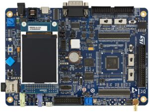
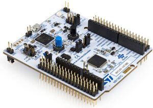
The best way to start experimenting with the STM32G4 is to use one of its development boards. We are releasing the NUCLEO-G474RE and NUCLEO-G431RB as well as the evaluation boards STM32G474E-EVAL1 ,STM32G474E-EVAL, and STM32G484E-EVAL. They all have a display while the STM32G474E-EVAL1 also has a hardware configuration for single and dual motor control and STM32G484E-EVAL integrates a crypto-core and a true random number generator. Finally, we are also offering a complete Nucleo pack for motor control applications (P-NUCLEO-IHM03) to accompany the release of a new version of X-CUBE-MCSDK, our new motor control Software Development Kit that will receive updates to take advantage of the new math units of the STM32G4, among other things.
- Check out the STM32G4
- Read the STM32G4 Press Release
