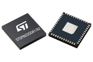
The low-voltage versions of the STSPIN32G0 are now available, thus vastly expanding the mainstream appeal of this new family of devices. The STSPIN32G0 is the first three-phase BLDC controller embedding an STM32G0 and a triple-half bridge gate driver capable of driving traditional power MOSFETs and IGBTs. In essence, it’s our first mainstream STSPIN32. It’s designed for applications that need more computing power than what’s available on the STSPIN32F0 but don’t require the high-performance features of the STSPIN32G4, thus ensuring a more cost-effective bill of materials. Hence, it can still run some advanced field-oriented control algorithms for applications needing less memory.
The mainstream challenge

Avid readers of the ST Blog know that the STSPIN32 family of devices stands out by integrating an MCU and a motor driver into one device. This saves costs and simplifies designs, resulting in a system up to 65% smaller. At a time when eBikes, robot vacuums, power tools, and consumer appliances must be more efficient and consumer-friendly, a smaller footprint is essential to fit bigger batteries and create more attractive products. However, the need to make more cost-effective systems that couldn’t fit into constrained MCUs grew as companies tried to reach new markets. The challenge was, therefore, to find the right compromise to ensure developers could run their applications while getting substantial savings.
The 2 versions of the STSPIN32G0
The high-voltage versions of the STSPIN32G0
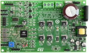
Meeting the needs of mainstream applications is one of the most complex technical challenges because constraints can widely vary. Hence, we made the STSPIN32G0 accessible to more designs by coming up with two versions: low-voltage and high-voltage. The STSPIN32G0251 and STSPIN32G0252 include a 250 V gate driver, while the STSPIN32G0601 and STSPIN32G0602 can handle up to 600 V. All four comprise the high-voltage family of devices that have been available since the introduction of the STSPIN32G0 earlier this year. Traditionally, these devices would target inverters for various applications, such as commercial or industrial appliances, and fans, given their high-voltage support and ability to provide up to 1 A to the gate driver.
The low-voltage versions of the STSPIN32G0
Today, we are extending our portfolio with the STSPIN32G0A1, STSPIN32G0A2, STSPIN32G0B1, and STSPIN32G0B2. All offer a voltage regulator and a gate driver rated at 45 V and up to 0.6 A. The A series includes three shunts, which means it can run six-step sensored or sensorless algorithms with accuracy, while the B series limits itself to one shunt, allowing the use of fewer external components.
Finally, the difference between the part numbers ending in “1” is that they have fewer pins than those finishing with “2” but they support Vbat to serve as a backup to the Vdd for critical components, thus ensuring the system can resume what it was doing after losing power or “Vref”, thus guaranteeing a precise reference for the ADC. All four devices target appliances, power tools, drones, and more.
The 1 vision of the STSPIN32G0
The same robustness and flexibility
As with the STSPIN32G4, all STSPIN32G0s integrate bootstrap diodes to reduce the need for external components further. The low-voltage versions also include the power management circuitry internally, generating 3.3 V for the microcontroller and 12 V for the gate driver. Hence, while the MCU and gate drivers target mainstream applications, ST still ensured that engineers would have access to advanced features and enjoy the same level of integration as with the high-performance version. In a nutshell, many products that can run their FOC algorithms on 8 KB of RAM and 64 KB of Flash and don’t require the CORDIC accelerator found in the STSPIN32G4 will easily gravitate toward the more cost-effective STSPIN32G0.
The positive feedback
In fact, some of the first design wins for the low-voltage versions of the STSPIN32G0 happened because customers had memory concerns. Developers had applications that would have had difficulty fitting in a more memory-constrained MCU. As we worked with them, they immediately adopted the new devices because they gave them the space they needed without blowing up their bill of materials. They appreciated the robustness, flexibility, and efficiency of the device. At the same time, the bigger memory size meant they didn’t have to spend significant development time on optimizations, thus enabling them to release to market faster.
The best way to get started

To help designers get started, we are shipping the EVLSPIN32G0A1/B1 evaluation board, which comes with 60 V MOSFETs and a feedback network to quickly get data from digital Hall sensors and the encoder’s input. The evaluation kit also supports three and single-shunt configurations to help teams choose the one that best suits their system. The new board is already compatible with X-CUBE-MCSDK, which will help developers implement six-step or FOC algorithms, among others. The new board thus augments the existing portfolio, which includes the EVSPIN32G02Q1S1 and EVSPIN32G06Q1S1, the 250 V and 600 V development boards for the high-voltage STSPIN32G0s.
