To improve the accessibility of our content, please find the audio version of this blog post.
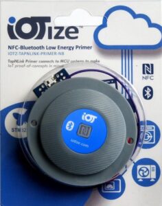
TapNLink, from the French company IoTize, an ST Authorized Partner, is the first RF module that directly connects to a microcontroller’s (MCU) debug port to facilitate development and offer an original approach to design. The product uses an ST25DV-I2C NFC tag to enable a mobile application to read and write on an MCU. TapNLink also combines NFC and Bluetooth Low Energy (BLE) so users can switch from one to the other when necessary. In a nutshell, IoTize offers a new way to interact with embedded systems.
How Did We Get to the NFC 3-Stroke Configuration Feature?
TapNLink officially launched in 2018, and it raised a few eyebrows because it turns foundational design principles on their heads. Traditionally, engineers develop an RF stack and create an application that will conform to complex standards. The process can be long, taxing, and often requires regulatory approvals. It can also be frustrating when managers expect their engineers to know everything about electronics, RF, antenna design, and a myriad of other fields that govern the transport of packets wirelessly from one device to the next. TapNLink bypasses all this by just grabbing data and propagating it. Indeed, IoTize offers a solution that handles many of these issues using NFC or Bluetooth so designers can focus on their applications.
The approach is so original it won Best Emerging Concept at the 2018 NFC Forum Innovation Awards. Since then, IoTize has continued to find new applications and make the technology even more accessible. Thanks to ST’s ST25DV, TapNLink’s NFC 3-Stroke Configuration is increasingly popular in trade shows and demo and won the Most Innovative Use of NFC award last year. The presentation was particularly successful in SIDO 2021 Lyon and should meet a similar fate next month in Paris. In a nutshell, customers talk to their appliances through the NFC tag. They first bring their phone close to the ST25DV, which will trigger an application on the user’s phone. The second step is to use the app to change settings and improve configurations. Finally, the third step involves bringing the phone back to the NFC Tag to register the new settings.
What New Applications Are Using TapNLink?
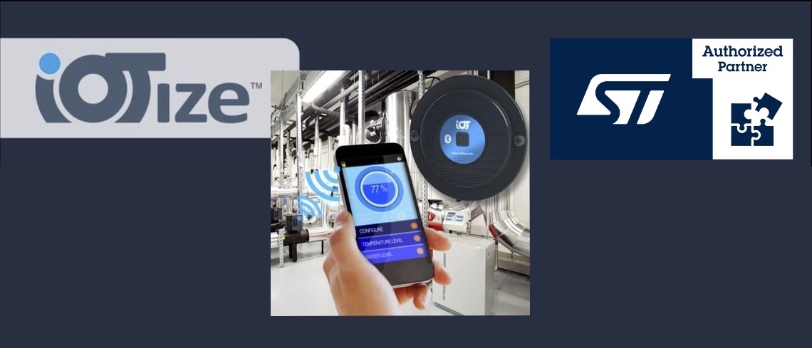
European consumers should start to see NFC 3-Stroke Configuration on heating appliances. Indeed, Cotherm, a French company, is working with IoTize to help users more easily configure their heaters. Improving the product’s interactivity will also help promote energy-saving features and lead to more significant environmental benefits. IoTize is also working with Lucht LHZ, a German manufacturer of electrical heaters. Additionally, TapNLink is gaining ground as an access control system. Indeed, the NFC solution interacts with a mobile application to grant or deny entry. Hence, users can expedite the process, and manufacturers can offer a more reliable solution. IoTize’s technology is also present in industrial monitoring solutions.
The new use cases stem from implementing the NFC 3-Stroke Configuration feature without writing a single line of code. Indeed, a new tool generates the application according to the STM32 microcontroller used, thus saving time and accelerating the release to market. IoTize also offers an automatic app generator for iOS and Android. The tool uses HTML5, CSS, and Javascript to create universal applications tailored to the settings users can change on their embedded application. Let us explore TapNLink in greater detail and see how it works behind the scenes.
TapNLink in Your Embedded System
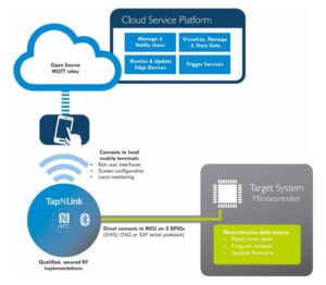
Connecting TapNLink to the debug port of an embedded system is the door to an almost instantaneous proof-of-concept on existing hardware. Engineers don’t need to write new stacks, change the PCB, or create a new design integrating NFC and BLE. They can take an existing product and plug in a TapNLink. As Francis Lamotte, Founder of IoTize and inventor of the concept, told us:
“TapNLink can compress the time scale that it takes to develop your proof-of-concept and move to an application. We are also inverting design principles, so the host machine becomes a target of the RF module and smartphone application to get data faster and more easily, without any major changes to the hardware or existing code.”
Beyond the Debug Port

Using the MCU’s debug port is sometimes impossible. In some instances, engineers must work with closed designs that can’t allow such operations. As a result, IoTize ensured that its product could connect to two General Purpose Inputs/Outputs (GPIOs), thus enabling teams to benefit from the same feature set, even if the debug port is unavailable. This method uses a “serial agent” similar to the debugging technology present on STM32 MCUs. Engineers will have to re-link the target firmware with IoTize’s “serial agent,” but it will only be a matter of hours. Moreover, this approach still means that developers don’t have to write new code for their systems.
Even if a TapNLink with NFC only does exist, most engineers will probably adopt the NFC-BLE Primer since Bluetooth Low Energy will facilitate the development of a prototype that can send data to a mobile terminal and demonstrate cloud features. On the other hand, for many local interactions with the system, using NFC is simpler. Indeed, when it comes to configuration or firmware updates, among other things, the ST25DV-I2C tag offers a more practical approach.
ST25DV-I2C in the TapNLink

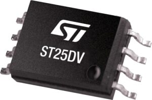
Our ST25DV NFC tags have a dynamic – also called dual – interface, meaning that, unlike traditional tags, it’s possible to use the module through the NFC or I2C protocols, which enables new applications that would have previously required more complicated and costly solutions. In the TapNLink, the dual interface is a middleman between the application reading the NFC tag and the MCU.
IoTize uses the 64 kb EEPROM version of the ST25DV-I2C. The memory stores a link to app stores, so users accessing the module for the first time automatically get the proper application without waking up the whole system or requiring more power than what the smartphone provides as it reads the NFC tag. The TapNLink also uses the tag’s internal memory to accelerate communication between the host MCU and the mobile device. Furthermore, the ST25DV-I2C provides a fast transfer mode. In a nutshell, its 256-byte buffer serves as a cache to optimize operations. Steve Gussenhoven, IoTize Marcom Manager, actually explained that:
“When we demo the TapNLink to the public, we find that the ST25DV-I2C is very responsive. Wake-up times are surprisingly fast, and it’s a tap-and-connect experience rather than a tap-hold-connect feeling. We did spend time optimizing and validating our antenna design to offer optimal performances to our customers, but it’d amount to nothing if the ST tag were slow.”
Security in Your Device

TapNLink takes care of the wireless modules, antenna design, and performance optimization, as well as one critical feature that engineering teams may overlook: security. There are inherent risks to using the debug port or connecting directly to an MCU’s GPIOs. When working on a proof-of-concept, the data transferred is usually harmless, meaning that security isn’t a major priority. However, it should never be an afterthought, which explains why IoTize is fond of the ST25DV-I2C. With our NFC tag, TapNLink can ensure that all wireless modules (NFC and BLE, for instance) are asleep to avoid sniffers. Hackers often use sniffers to detect active wireless networks before checking for vulnerabilities. The Bluetooth module is also up if the user reads the NFC Tag and exchanges encryption keys.
Another feature that makes the TapNLink practical is the Simulated Secure Serial Port, or S3P, which works as an alternative to Arm’s Serial Wire Debug interface (SWD). Any developer with experience in embedded systems will most likely be familiar with the latter. It allows direct communication through the debug port to access the memory map quickly, among other things. The problem is that SWD offers no encryption scheme. Even Arm recommends a dedicated logic in the form of a Debug Authentication Module, which isn’t always present or practical. Alternatively, TapNLink provides S3P to secure data exchanges between the IoTize module and the MCU using an AES–128 scheme. The technology also filters memory addresses to reduce the risk of a mishap. Moreover, the device uses the internal RAM of the ST25DV-I2C to exchange dynamic keys, further optimizing security operations.
Where to Start?
A great way to start using the TapNLink is to get an evaluation kit called the TapNLink Primer, which supports NFC, Bluetooth Low Energy, and costs €59 online. Aside from the hardware, IoTize also offers a cloud platform to start experimenting with remote features immediately. Additionally, the TapNLink Primer uses an open source MQTT relay to connect to most cloud service providers.
