ST will be presenting three papers at the VLSI 2021 Technology and Circuits Symposiums, two on the largest embedded phase-change memory (PCM) for automotive, and one on a new on-chip DC-DC converter made of stacked LC oscillators shaped like the number eight. We thus sat down with some of the authors to better understand why VLSI 2021 chose their work and the impacts of their research on the industry. Indeed, what makes these contributions unique is that they shine a spotlight on FD-SOI. For instance, the two papers on the new PCM were only possible thanks to FD-SOI substrates. Similarly, ST is using FD-SOI to shrink the new on-chip DC-DC converter. While many devices benefit from FinFET technologies, these findings show FD-SOI still plays a significant role today. Let us, therefore, explore these advances a little further.
VLSI 2021 Circuits and Technology: Phase-Change Memory
The Largest Embedded Auto-Grade PCM Today

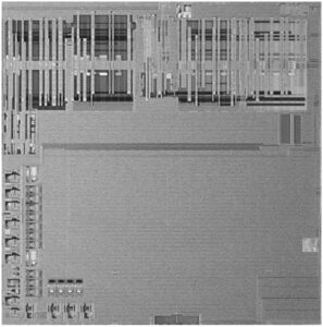
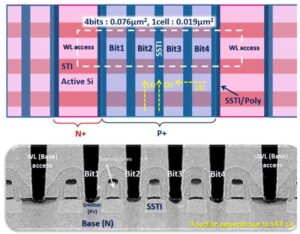
Fabio Disegni will present a new 28-nm embedded PCM with a capacity of 16 MB. Due to the stringent reliability requirements of the automotive industry, each logical bit uses two memory cells for redundancy’s sake. Hence, it is theoretically possible to increase the capacity even further by using only one cell per bit. Regardless, the innovation is highly symbolic because ST now offers a cell size of only 0.019 µm2 in an embedded non-volatile memory. Previously, engineers had to use discrete memory modules to obtain such a density. Furthermore, the paper is detailing a memory technology that ST already qualified and is sampling. Put simply, engineers can expect commercial devices to use this technology within the year.
Fabio’s paper, which will be part of VLSI 2021 Circuits, explains what engineers can expect from the new memory. ST measured its random-access time at 10 ns, which is on par with previous models. However, given the vastly superior capacity, we are looking at a theoretically read throughput of 166 Gbit/s. The paper also describes an over-the-air memory configuration for updates that increases capacity to 24 MB. Hence, designers may switch between redundancy or increased capacity depending on their application. As a result, developers get a higher density embedded phase-change memory and a more flexible architecture.
The Most Advanced Auto-Grade PCM Today

Olivier Weber, Principal Engineer at ST, will present a paper at VLSI 2021 Technology that explains how we managed to create our new 16 MB embedded PCM module at 28 nm. His presentation is thus a complementary exposition that delves into the innovations that went into isolating the bipolar-junction transistor (BJT) responsible for heating the chalcogenide compound. Indeed, to write a PCM cell, the system applies a voltage to a BJT, which heats the compound to change its state. An amorphous state is highly resistive and represents a logic 0. A polycrystalline phase is highly conductive and represents a logic 1. Moving from one to the other is simply a matter of sending the proper voltage to the BJT. Isolating it is, therefore, of the utmost importance.
In discrete modules, manufacturers isolate the BJT thanks to a process called Super Shallow Trench Isolation (SSTI). Olivier’s paper is a breakthrough because it shows how ST, for the first time in the industry, applies this process to embedded PCM. To achieve this, we are using the buried oxide of the FD-SOI substrate to create an isolation wall between the bitlines, which prevents bitline-to-bitline leakage. Additionally, the ST paper shows that it is possible to use the same process to shrink the embedded cell to 0.015 µm2, from 0.019 µm2 today. The technology is thus highly scalable and should further help democratize phase-change memory modules.
VLSI 2021 Technology: On-Chip DC-DC Converter
Mathieu Coustans, RF Analog Designer at ST, will finally present another paper at VLSI 2021 Technology in partnership with ETH Zurich featuring a DC-DC converter made of vertically stacked transformers shaped like the number eight. Despite the embedded nature of the converter, it provides an interesting efficiency and a wide range of operating voltages (from 0.8 V to 3 V). ST is still working on implementing the technology in commercial devices. Hence, it is too early to talk about mass production. Yet, the paper shows promising results at 22 nm when using an FD-SOI wafer. Indeed, the research currently demonstrates a peak efficiency of 78.1% at 0.2 W/mm<sup>2</sup>.
ST and ETH Zurich achieved this level of performance by stacking two class-D LC oscillators that are then electrically and magnetically coupled. The design vastly reduces ripples without needing an output capacitor, and its magnetic field is more contained (only 58 dBm/µV vs. 85 dBm/µV for a traditional loop transformer), thus reducing EMIs. The reason is that the passive devices are coupled with each other but not the rest of the circuit. The architecture also enables smaller gate capacitance, which explains in part the increase in power density. Consequently, even if the converter’s on-die footprint may be slightly more voluminous, it contributes to the use of smaller packages.
