
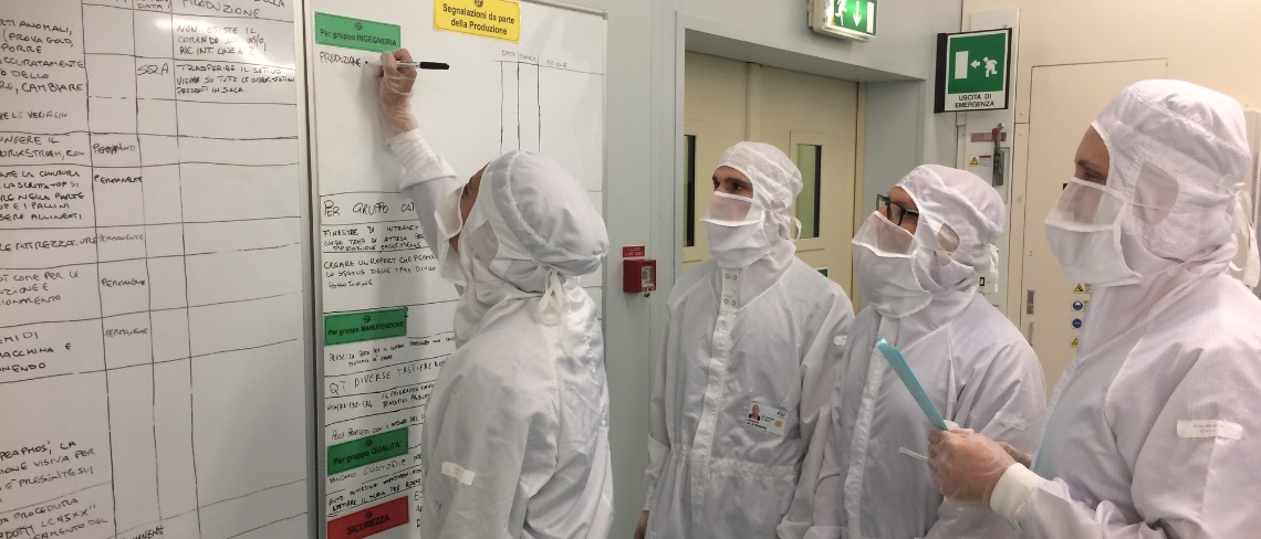
ST is announcing Lab-in-Fab 2.0, an expansion of the “Lab-in-Fab” initiative launched in 2020 that now includes new projects with Singapore’s A*STAR Institute of Materials Research and Engineering (A*STAR IMRE) and the National University of Singapore (NUS). Located within ST’s Singapore Ang-Mo-Kio campus, Lab-in-Fab is an 8-inch (200 mm) facility. The expansion will enable more startups and companies to advance piezoelectric MEMS and increase their popularity by reducing the time to market from a proof-of-concept to mass production. Put simply, this new milestone expands the scale and scope of Lab-in-Fab, making it more accessible and increasing its impact on the tech market.
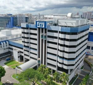
Lab-in-Fab was the world’s first 8-inch (200 mm) ST manufacturing facility in Singapore with a twist. It also houses the A*STAR research institute and the Japanese manufacturing-tool vendor ULVAC. Together, we combined R&D and high-volume manufacturing capabilities so engineers could bring concepts to life faster. Companies benefit from theoretical and practical expertise in one place to transform the piezoelectric MEMS market. And, according to professors from Peking University, ShanghaiTech University, and the Taiwan Semiconductor Research Institute, Lab-in-Fab 1.0 worked! They shared how it positively impacted their research, thanks to deliveries of prototypes in just a couple of months instead of two to three times that, thanks to multi-project wafers (MPW).
Understanding piezoelectric MEMS and the innovation challenge
What are piezoelectric MEMS?
To understand the challenges behind piezoelectric MEMS, managers and decision-makers must grasp what they are. At their core, they are micro-electro-mechanical systems that take advantage of the piezoelectric effect. The latter describes the generation of an electrical charge when applying mechanical stress on certain materials and vice versa. According to the Bhugra and Piazza textbook1, the first thin-film piezoelectric resistor dates back to 1981 and used zinc oxide. Today, most piezoelectric MEMS use lead zirconate titanate (PZT) chemical deposition. The material enabled the creation of smaller devices compatible with micromachining. Today, the most common applications are in audio markets with piezoelectric transducers in MEMS microphones, for instance.
Where are piezoelectric MEMS?

The world of piezoelectric MEMS is increasingly vast. While most experts think of MEMS speakers and microphones, there are many more applications. Some devices serve as gyroscopes or accelerometers, while others act as micromirrors or particle detectors. There are also piezoelectric MEMS used for infrared detection that work by exposing lanthanum-doped lead zirconate titanate (PLZT) to infrared, for example, which leads to a change in temperature that then generates an electrical charge. However, there are a lot of fields of research that still need considerable work, and Lab-in-Fab offers a unique opportunity to break new ground.
What are the challenges inherent to piezoelectric MEMS?
If piezoelectric MEMS aren’t new, they remain particularly challenging to make, which slows their adoption. As devices get smaller, designers sometimes struggle with the signal-to-noise ratio. Engineers must also ensure that their system works flawlessly regardless of temperature or other environmental fluctuations. Similarly, coming up with MEMS that can stand the test of time is just as tricky. In a nutshell, piezoelectric MEMS still face some steep challenges if they are to become even smaller and more cost-effective. To find the correct answers, the industry will need material research and important manufacturing optimizations. Hence, Lab-in-Fab is a unique solution because it brings all the actors working on these problems under one roof.
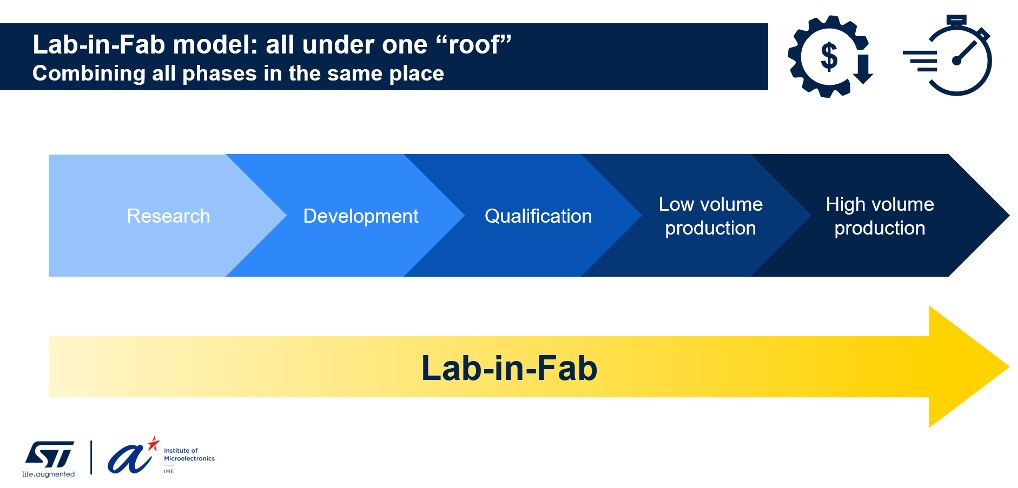
Discovering Lab-in-Fab as the driver of piezoelectric MEMS innovation
A direct path to high volume manufacturing
Too often, MEMS and sensor companies underestimate the expertise and investments it takes to go from concept to high-volume production. Many suffer from delays and high development costs because of unexpected issues during the prototyping phase or an inability to scale their production. Additionally, very few facilities can handle everything in-house. Consequently, makers use multiple plants, which can create further delays and add to the overall complexity. Put simply, many struggle to find the right industrialization partner that can support them efficiently from their early-stage research all the way to their mass market launch.
Having ST, A*STAR, and ULVAC together means that clients can work with a broader range of experts. Moving from R&D to production is easier. Similarly, optimizing high-volume manufacturing, which is a vital issue in this field, will also be more straightforward. Too often, industry actors work with educational institutions at a very theoretical level. As a result, too few papers ever get a chance at high-volume production and real-world applications. Lab-in-fab tackles this issue by offering a direct path from “thesis-to-metamorphosis””.
The need for greater flexibility
Additionally, researchers continually devise new tools and ideas. Unfortunately, they often lack the necessary equipment or facilities for testing. Lab-in-Fab offers a unique approach to experimentation. Similarly, the project provides significant flexibility by allowing some clients to utilize Lab-in-Fab solely to address specific challenges. We are, therefore, committing to being as flexible as possible to help engineers overcome new issues rather than being tied to infrastructure.
In essence, the primary objective of this facility is to establish itself as a global leader in microsystems research while supporting customers in their journey to the industrialization of leading-edge sensor and actuator products. Through Lab-in-Fab, customers have the unique opportunity to develop advanced products using state-of-the-art R&D facilities, all embedded in a high-volume-capable facility, accelerating their time to volume production. By combining world-class R&D personnel, key semiconductor equipment, and access to the complete IME’s and ST’s development ecosystem, Lab-in-Fab provides an expanded set of services for companies seeking to develop and manufacture MEMS-based products.
The desire for better opportunities
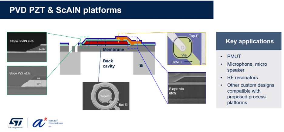
As we explained, piezoelectric-based MEMS (PZT, AlN, ScAlN) are one of the core technological platforms available within Lab-in-Fab. This is only possible because the PiezoMEMS platform is the result of years of accumulated expertise in material optimization, which has enabled many successful product launches. And now, thanks to Lab-in-Fab, this same expertise is helping our customers develop innovative applications in domains such as Piezoelectric Micromachined Ultrasonic Transducers (PMUT) for emerging medical applications, MEMS-based microphones, micro-speakers, RF resonators/filters, and more. Moreover, we recently launched an MPW service to provide external partners with dedicated access to state-of-the-art piezoelectric thin-film developments.
We are also thrilled to work with a partner looking to use piezoelectric MEMS in AR and VR applications. Indeed, Lab-in-Fab is already trying to make glasses and headsets more comfortable for very long periods, thus opening the door to a viable metaverse experience. It is currently possible to apply to join Lab-in-Fab. At this point, ST, A*STAR, and ULVAC are looking for companies with the expertise to take advantage of this initiative.
Finally, ST reached out to smaller companies. Many say they sometimes feel left out of initiatives like Lab-in-Fab. As a result, we created ST for Startups, a program specifically designed for emerging companies. Once accepted, startups gain access to ST experts, advanced manufacturing innovations, and assistance in developing new IP. Thanks to multi-project wafers, they also get the latest technologies and platforms that Lab-in-Fab has to offer, enabling them to create rapid proof-of-concepts, test feasibility, and more. They can even leverage ST’s marketing activities to shine a brighter light on their project.
- Harmeet Bhugra, Gianluca Piazza. Piezoelectric MEMS Resonators. p. 283. https://doi.org/10.1007/978–3–319–28688–4 ↩︎