Discover the latest STPOWER wide bandgap transistors
Should engineers adopt Gallium Nitride (GaN) power devices, or is it still too early? Part of the answer lies in our recent acquisition of a majority stake in Exagan, a French innovator with unique epitaxial growth expertise and one of a select few to enable the mass deployment and production of GaN power devices on 8-inch (200 mm) wafers. The investment in Exagan by ST is a continuation of our long-term commitment in compound power semiconductors. Indeed, we recently launched MASTERGAN1, the first 600 V system-in-package with a gate driver and two enhancement-mode GaN transistors in a half-bridge topology. The device opens the door to cost-effective power supplies for laptops and smartphones, among other things. As a result, engineers are increasingly viewing the design and production of GaN power devices as mainstream.
The Importance of Being First
Gallium Nitride is a compound III/V semiconductor material. It has a wide bandgap of 3.4 eV and an electron mobility of 1,700 cm2/Vs. Comparatively, Silicon sits at 1.1 eV and 1,400 cm2/Vs. GaN’s inherent properties thus result in a higher breakdown voltage and lower on-state resistance, which means that the component can more efficiently handle greater loads compared to a similar-sized silicon device, which then leads to a lower bill of materials. ST, seeing GaN’s potential, was one of the first companies to provide mainstream power devices featuring the new material. Indeed, the MASTERGAN series offers the first and only system-in-package in the industry with two e-Mode GaN transistors.
And now, the agreement with Exagan means ST will be the first company to have depletion-mode (D-mode) and enhancement-mode (E-mode) GaN devices in its portfolio. D-mode high electron mobility transistor (HEMT) use a “normally-on” die configuration, meaning that they have a naturally conducting channel that doesn’t require the application of a voltage at the gate. D-mode represents the natural form of GaN-based devices and it often integrates a low-voltage Silicon MOSFET in a Cascode configuration. On the other hand, “normally-off” or E-mode devices have a P-GaN channel that requires a voltage at the gate to be conductive. Both are increasingly present in consumer, industrial, telecom, and automotive applications.
The Adoption Dilemma

Despite the increased popularity of GaN devices, problems may arise when engineers meet reluctant managers or manufacturing partners. On the one hand, even end users are starting to learn about Gallium Nitride. GaN power devices are increasingly present in everyday items, as we showed during the Industrial Summit 2020. Additionally, popular tech media, like Engadget or The Verge, among others, are doing a great job at explaining GaN’s benefits. On the other hand, certain makers of industrial products, for instance, may avoid GaN for fear of a potential PCB redesign or sourcing issues. Let us, therefore, explore the impact of the ST and Exagan solutions to help engineers better grasp where GaN now fits in their products and operations.
ST and Exagan: Accelerating GaN’s Large Scale Adoption
The Importance of Larger Wafers
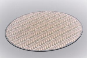
A new technology can only reach massive adoption if it is possible to manufacture it effectively. At the turn of the century, the industry still struggled with a such a high number of defects in Gallium Nitride crystals that devices were unviable. Things have greatly improved since then. Yet, engineers can only realistically envision using GaN power devices if manufacturing processes continue to improve. Exagan’s work was thus highly symbolic because the company increased yields while also using 8-inch wafers. As Eric Moreau, Product and Application Director at Exagan responsible for coordinating the PowerGaN systems and application ecosystem explained,
The Importance of Using Current CMOS Fabs

Regardless of the technology, engineers must have the assurance that the components they need will be available. Indeed, teams will inevitably wonder if they can count on GaN power devices, especially when dealing with high volumes. With Exagan’s technology, epitaxial process, and expertise, ST is now fitting this technology into its current fabs without any extraordinary investment in unique tooling equipment. Plants can thus enjoy greater yields and ramp up production faster. The industry can therefore expect greater cost-effective solutions and more reliable supply chains.
ST and Exagan: What ST’s PowerGaN Means for the Industry
The Groundwork for Today
Engineers looking to convince their managers must demonstrate GaN’s value proposition. Theoretical numbers are great, but decision-makers demand real-world values. One way teams are solving this challenge is by showing the circuit’s performance. Indeed, GaN devices enable a drastic reduction of both conduction and switching losses, which in turn lowers the cooling system’s bill of materials. Additionally, the better switching performance implies smaller and lighter passive components, i.e., capacitors and inductors. As a result, engineers can create significantly more compact systems (up to four times) thanks to a higher power density. Hence, even if GaN devices may be more expensive compared to Silicon alternatives (MOSFET or IGBT), the benefits they bring tip the scale in their favor.
With the Exagan integration, ST will have among the strongest GaN IP portfolio in the market because we’ll be capable of offering both E-mode and D-mode GaN products, thus showing a clear roadmap into the next decade. As Roberto Crisafulli, GaN Business Unit Manager at ST explained
A Foundation for the Future
Forty years ago, Silicon became ubiquitous in electronics because the industry started using it efficiently and reliably in transistors. And it’s from such a foundation that all other innovations in Silicon devices still flow today. Manufacturers can’t justify moving a technology forward if they can’t already see some positive results. By combining ST’s and Exagan’s technologies, we created a solid foundation for future GaN investments and innovations. Put simply, Gallium Nitride is today where Silicon was forty years ago, and the industry has but glimpsed at its growth potential.
- Learn more about ST’s GaN initiative
- Check out Exagan
