The STM32H7A3, STM32H7B3, and STM32H7B0 are the first STM32 microcontrollers to embark 1.4 MB of RAM, and they offer the lowest power consumption of the entire STM32H7 series with a STOP mode demanding only 32 µA. The lower power consumption of the new models was partly possible thanks to their single Cortex-M7 at 280 MHz and the presence of a new power supply. These new models thus target engineers that are looking for the features of the STM32H7, such as the double-precision FPU or its plentiful I/Os, but want a lower power consumption as well as the greater integration that the more significant memory affords. The new components are a great addition to the STM32H7 series because they open these MCUs to new applications.
The latest devices are highly symbolic because they are a new chapter in the history of the STM32H7 series. When we introduced it in 2016, it was the first-ever to break the 2000-point threshold in CoreMark. Last year, we achieved a new milestone by introducing STM32H7s that were also the first dual-core STM32s ever. Today’s devices represent a break from the power race to address designers searching for efficiency and integration. The only difference between the STM32H7A3 and STM32H7B3 is the presence of a crypto core on the latter. While they both have up to 2 MB of Flash, the STM32H7B0 has 128 KB since it targets engineers that want as little embedded storage as possible since they’ll use an external Flash anyway. The STM32H7A3 and STM32H7B3 are available today, while the STM32H7B0 will land during the second quarter of 2020.
STM32H7A3, STM32H7B3, and STM32H7B0 Boost Graphical Interfaces
More SRAM

These new MCUs respond to an upcoming trend: the rise of GUIs in embedded systems. 1.4 MB of SRAM can store an entire frame buffer, which means that designers don’t have to rely on slower external memory. Moreover, out of the 1.4 MB available, 1 MB is contiguous, which improves overall latency and further helps performance in graphical applications. For STM32H7B0 systems that use external storage, the MCU no longer has to share the memory bandwidth between the code and graphics. The system can store the graphics in the internal RAM while running the program from the external Flash.
Chrom-GRC
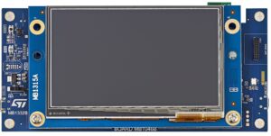
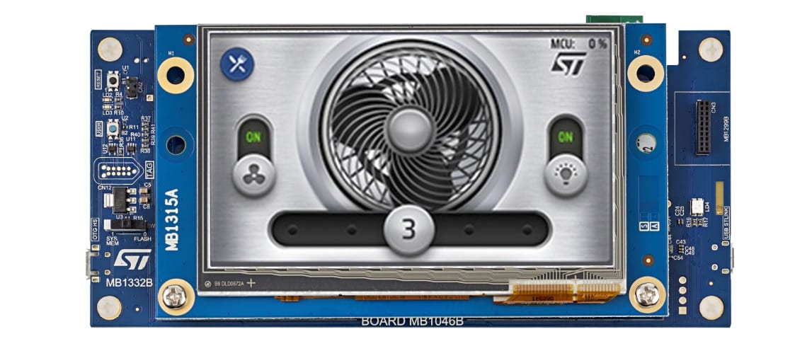
These new models are the first STM32H7s to get Chrom-GRC (Graphics Resource Cutter), a hardware unit we introduced with the STM32L4+ that shrinks the frame buffer by up to 20% when using a round display, such as those present on a smartwatch. To save resources, Chrom-GRC discards pixels that won’t be visible due to the shape of the screen. Moreover, the TouchGFX Generator already supports the new devices as well as the STM32H7B3 Discovery board, so engineers can quickly benefit from these features.
Octo-SPI

To further help teams that are looking to offer richer graphics, we included a dual Octo-SPI interface. It’s high throughput and memory-mapped mode means that external Flash is treated as an internal memory during read operations while the low pin count makes designing a PCB simpler. For instance, it’s possible to include both a fast HyperRAM and a Flash storage for better performance, map each of them to their respective Octo-SPI port, and use the available multiplexed mode to limit the number of pins necessary, thus greatly simplifying the overall design.
STM32H7A3, STM32H7B3, and STM32H7B0 Improve Security and Efficiency
On-the-Fly Decryption (OTFDEC)
The new crypto core available on the models with a “B” in their nomenclature now supports the decryption of AES 128 bit data on the fly to prevent any latency during cryptographic operations. Its primary purpose is to allow developers to use encrypted code inside their external memory without incurring any penalty. Traditionally, an encrypted program must reside on the internal memory to prevent it from negatively impacting performances. With OTFDEC, engineers can better protect the IPs they put on their external memory.
OTFDEC adds to the security features of the STM32H7 that are also part of the STM32Trust Program, our latest initiative designed to bolster security on embedded systems. Users can use the STM32H7 crypto core to accelerate cryptographic operations, protect their firmware from malicious attacks with SecureBoot, and guard their IP thanks to the embedded secure elements that enable the creation of a Root of Trust. The presence of a RoT means developers can ship encrypted applications or firmware that will only be decrypted by the MCU. It enables features like secure firmware install (SFI), secure firmware update (SFU), and secure module install (SMI), our latest security measures on the STM32H7. Companies thus protect their users and their intellectual properties by encrypting their code before sending it to third parties that rely on the ST tools to authenticate it, decrypt it, and load it in a secure fashion.
Smaller Clusters

The Flash memory now embedded in the STM32H7B0 has a much smaller sector size of only 8 KB instead of 128 KB previously. Shrinking the memory sectors offers a lot more granularity and opens the doors to features such as over-the-air firmware updates or the presence of a boot sector since it’s now possible to have a lot more flexibility than when there was only one larger sector. Developers can, therefore, make more efficient use of the internal Flash.
SMPS
Finally, the STM32H7A3, STM32H7B3, and STM32H7B0 integrate a new switched-mode power supply on top of the LDO already present in the STM32H7 architecture. The changes in the components’ power management, as well as the lower frequency and multiple architectural optimizations, explain the drastically lower consumption. The SMPS allows for more dynamic control of the electrical current to vastly improve the overall efficiency.
