

Power designs now face the same demands at the same time: higher efficiency, smaller size, lower cost, and more power from the same space. For years, silicon has supported these designs. However, in a growing number of applications, it is close to its practical limits, and further optimization increases losses and heat.
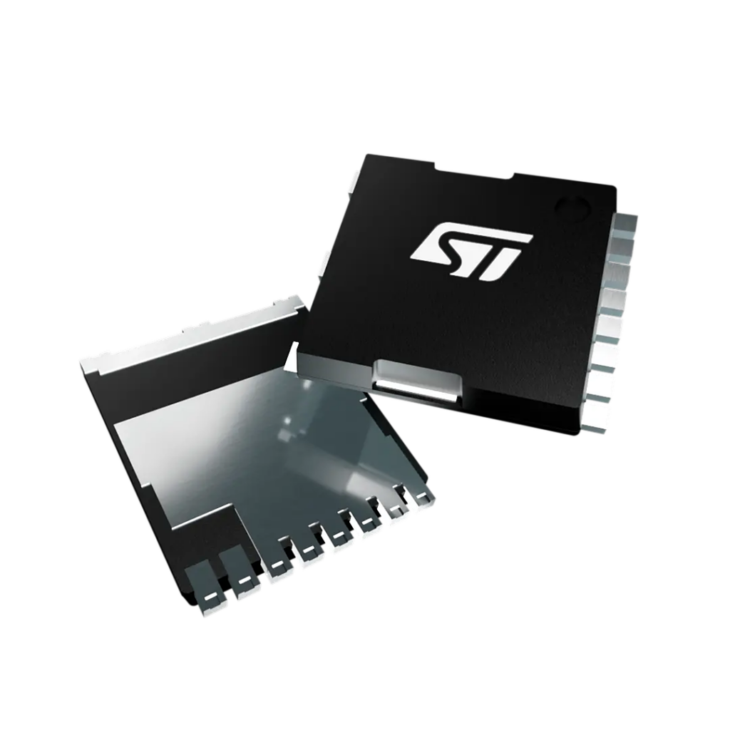
For this reason, gallium nitride (GaN) power transistors are receiving significant attention. ST has added a new 700 V and 100 V PowerGaN family to its portfolio and brings these advantages to mainstream power conversion. This article explains what the technology offers power designs and why it matters now.
Why use GaN power transistors
Gallium nitride is a wide-bandgap semiconductor and, in a power converter, its main advantage is speed. Gallium nitride (GaN) power transistors, also called gallium nitride high electron mobility transistors (GaN HEMTs), switch much faster than silicon devices and lose less energy each time they turn on and off. Two effects follow from this behavior. Less energy is wasted as heat, and the converter can operate at a higher switching frequency without losses increasing as they do with silicon. Almost every benefit of GaN results from these two effects. Until recently, the technology appeared mainly in specialized, high-end products where the cost was justified. With a broad 700 V to 100 V family now in production, GaN has become a practical choice for everyday power conversion across a wide range of designs.
Improved efficiency
The clearest benefit is efficiency. Because GaN has low conduction and switching losses, more of the input power reaches the load, and less of the power turns into heat. In ST reference designs, PowerGaN has achieved power-supply efficiency of up to 98.6%. Higher efficiency affects the entire design: lower operating costs, less energy consumption over the product life cycle, and lower demand on the cooling system. For equipment that operates continuously, such as power supplies, lighting, and energy systems, even a small efficiency gain accumulates over thousands of operating hours. Efficiency is usually the first reason that a design team considers GaN, and it leads directly to the next two benefits.
Increased power density
The second benefit is size. A higher switching frequency allows the bulky magnetic components and filters in a converter to shrink, and the rest of the design shrinks with them. That creates two options for a design team: deliver the same power in a smaller, lighter product, or fit more power into an existing enclosure. Gallium nitride (GaN)-based designs have reached an average size reduction of around 50%, compared with earlier silicon equivalents, at power densities above 100 watts per cubic inch. For products with tight space and weight constraints, such as compact adapters, chargers, and on-board systems, that extra headroom can determine whether a design fits at all. Increased power density is where the move to GaN becomes visible in the finished product.
Reduced system cost
The third pillar is lower system cost. It results as much from the design around the transistor as from the device itself. A gallium nitride (GaN)-based converter uses smaller passive components and fewer passive components and often requires little or no heat sink. As a result, the overall system cost decreases, and the design is simpler. Cooler operation also improves reliability and life cycle, which means that the system tends to last longer and requires less servicing. Lower energy consumption over the product life cycle adds to the savings. Together, these effects reduce the cost of building and operating the system, and they are a large part of why GaN deserves its place in a design.
Where 700 V & 100V PowerGaN fits
These benefits are not tied to a single product type. The same value higher efficiency, greater density, and lower total cost) extends across a broad range of designs, including AC-DC and DC-DC power supplies, USB Type-C® adapters and chargers, LED lighting, motor control, AI servers, robotics, industrial systems, and advanced consumer applications such as home appliances, as well as power and energy systems such as solar and storage. The same value also supports the growing power demands of computing and electrification.
Across these areas, priorities differ, but the same three advantages apply. A choice of package options allows a design team to match the device to the power level and board layout of each application. Because the 700 V & 100V PowerGaN family is already in production and available, these benefits can already be built into designs today.
Backed by a broad portfolio
Adopting a new switching technology is a decision about support as much as about the device itself. Alongside the 700 V and 100 V family, ST brings decades of power semiconductor experience, a broad product portfolio, a reliable supply chain, and strong technical support. For a team that works with GaN for the first time, that combination reduces the risk of the transition and shortens the path from an idea to a working design. It is part of what makes the value of PowerGaN practical rather than theoretical.
Why GaN, and why now
GaN power transistors provide higher efficiency, greater power density, and lower system cost for power conversion. The new 700 V and 100 V PowerGaN family makes these benefits available to mainstream designs. For a design team that is considering the move to GaN, the technology has reached the point at which its advantages are practical today rather than promised for tomorrow.